RM46L450
RM46L850
SPNS184 –SEPTEMBER 2012
www.ti.com
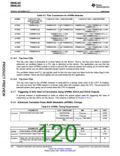
Table 5-3. TZ4n Connections for ePWMx Modules
ePWMx
Control for TZ4n =
Control for TZ4n = not(EQEP1ERR)
Control for TZ4n = not(EQEP2ERR)
not(EQEP1ERR OR
EQEP2ERR)
ePWM1
ePWM2
ePWM3
ePWM4
ePWM5
ePWM6
ePWM7
PINMMR41[0] = 1
PINMMR41[8]
PINMMR41[16]
PINMMR41[24]
PINMMR42[0]
PINMMR42[8]
PINMMR42[16]
PINMMR41[0] = 0 AND PINMMR41[1] PINMMR41[0] = 1 AND PINMMR41[1] = 0 AND
= 1 PINMMR41[2] = 1
PINMMR41[8] = 0 AND PINMMR41[9] PINMMR41[8] = 1 AND PINMMR41[9] = 0 AND
= 1
PINMMR41[10] = 1
PINMMR41[16] = 0 AND
PINMMR41[17] = 1
PINMMR41[16] = 1 AND PINMMR41[17] = 0
AND PINMMR41[18] = 1
PINMMR41[24] = 0 AND
PINMMR41[25] = 1
PINMMR41[24] = 1 AND PINMMR41[25] = 0
AND PINMMR41[26] = 1
PINMMR42[0] = 0 AND PINMMR42[1] PINMMR42[0] = 1 AND PINMMR42[1] = 0 AND
= 1 PINMMR42[2] = 1
PINMMR42[8] = 0 AND PINMMR42[9] PINMMR42[8] = 1 AND PINMMR42[9] = 0 AND
= 1
PINMMR42[10] = 1
PINMMR42[16] = 0 AND
PINMMR42[17] = 1
PINMMR42[16] = 1 AND PINMMR42[17] = 0
AND PINMMR42[18] = 1
5.1.6.3 Trip Zone TZ5n
This trip zone input is dedicated to a clock failure on the device. That is, this trip zone input is asserted
whenever an oscillator failure or a PLL slip is detected on the device. The application can use this trip
zone input for each ePWMx module in order to prevent the external system from going out of control when
the device clocks are not within expected range (system running at limp clock).
The oscillator failure and PLL slip signals used for this trip zone input are taken from the status flags in the
system module. These are level signals are set until cleared by the application.
5.1.6.4 Trip Zone TZ6n
This trip zone input to the ePWMx modules is dedicated to a debug mode entry of the CPU. If enabled,
the user can force the PWM outputs to a known state when the emulator stops the CPU. This prevents the
external system from going out of control when the CPU is stopped.
5.1.7 Triggering of ADC Start of Conversion Using ePWMx SOCA and SOCB Outputs
A special scheme is implemented in order to select the actual signal used for triggering the start of
conversion on the two ADCs on this device. This scheme is defined in Section 5.4.2.3.
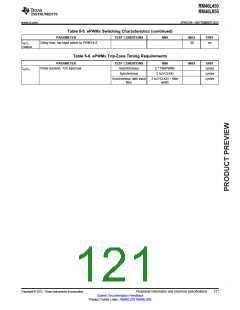
5.1.8 Enhanced Translator-Pulse Width Modulator (ePWMx) Timings
Table 5-4. ePWMx Timing Requirements
PARAMETER
TEST CONDITIONS
Asynchronous
MIN
MAX
UNIT
cycles
cycles
cycles
tw(SYNCIN)
Synchronization input pulse width
2 tc(VCLK4)
2 tc(VCLK4)
Synchronous
Synchronous, with input 2 tc(VCLK4) + filter width
filter
Table 5-5. ePWMx Switching Characteristics
PARAMETER
TEST CONDITIONS
MIN
33.33
MAX
UNIT
ns
tw(PWM)
Pulse duration, ePWMx output high or low
tw(SYNCOUT Synchronization Output Pulse Width
8 tc(VCLK4)
cycles
)
td(PWM)tza
Delay time, trip input active to PWM forced high,
no pin load
25
ns
OR Delay time, trip input active to PWM forced
low
120
Peripheral Information and Electrical Specifications
Copyright © 2012, Texas Instruments Incorporated
Submit Documentation Feedback
Product Folder Links: RM46L450 RM46L850

 TI [ TEXAS INSTRUMENTS ]