RM46L450
RM46L850
www.ti.com
SPNS184 –SEPTEMBER 2012
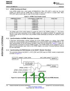
5.1.4 Phase-Locking the Time-Base Clocks of Multiple ePWM Modules
The TBCLKSYNC bit can be used to globally synchronize the time-base clocks of all enabled ePWM
modules on a device. This bit is implemented as PINMMR37 register bit 1.
When TBCLKSYNC = 0, the time-base clock of all ePWM modules is stopped. This is the default
condition.
When TBCLKSYNC = 1, all ePWM time-base clocks are started with the rising edge of TBCLK aligned.
For perfectly synchronized TBCLKs, the prescaler bits in the TBCTL register of each ePWM module must
be set identically. The proper procedure for enabling the ePWM clocks is as follows:
1. Enable the individual ePWM module clocks (if disable) using the control registers shown in Table 5-1.
2. Configure TBCLKSYNC = 0. This will stop the time-base clock within any enabled ePWM module.
3. Configure the prescaler values and desired ePWM modes.
4. Configure TBCLKSYNC = 1.
5.1.5 ePWM Synchronization with External Devices
The output sync from EPWM1 Module is also exported to a device output terminal so that multiple devices
can be synchronized together. The signal pulse is stretched by eight VCLK4 cycles before being exported
on the terminal as the EPWM1SYNCO signal.
5.1.6 ePWM Trip Zones
The ePWMx modules have six trip zone inputs each. These are active-low signals. The application can
control the ePWMx module response to each of the trip zone input separately. The timing requirements
from the assertion of the trip zone inputs to the actual response are specified in Section 5.1.8.
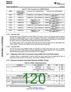
5.1.6.1 Trip Zones TZ1n, TZ2n, TZ3n
These three trip zone inputs are driven by external circuits and are connected to device-level inputs.
These signals are either connected asynchronously to the ePWMx trip zone inputs, or double-
synchronized with VCLK4, or double-synchronized and then filtered with a 6-cycle VCLK4-based counter
before connecting to the ePWMx. By default, the trip zone inputs are asynchronously connected to the
ePWMx modules.
Table 5-2. Connection to ePWMx Modules for Device-Level Trip Zone Inputs
Trip Zone Input
Control for
Asynchronous
Control for Double-Synchronized
Connection to ePWMx
Control for Double-Synchronized and Filtered
Connection to ePWMx
Connection to ePWMx
TZ1n
TZ2n
TZ3n
PINMMR46[16] = 1
PINMMR46[24] = 1
PINMMR47[0] = 1
PINMMR46[16] = 0 AND
PINMMR46[17] = 1
PINMMR46[16] = 0 AND PINMMR46[17] = 0
AND PINMMR46[18] = 1
PINMMR46[24] = 0 AND
PINMMR46[25] = 1
PINMMR46[24] = 0 AND PINMMR46[25] = 0
AND PINMMR46[26] = 1
PINMMR47[0] = 0 AND PINMMR47[1] PINMMR47[0] = 0 AND PINMMR47[1] = 0 AND
= 1 PINMMR47[2] = 1
5.1.6.2 Trip Zone TZ4n
This trip zone input is dedicated to eQEPx error indications. There are two eQEP modules on this device.
Each eQEP module indicates a phase error by driving its EQEPxERR output High. The following control
registers allow the application to configure the trip zone input (TZ4n) to each ePWMx module based on
the application’s requirements.
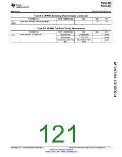
Copyright © 2012, Texas Instruments Incorporated
Peripheral Information and Electrical Specifications
Submit Documentation Feedback
Product Folder Links: RM46L450 RM46L850
119

 TI [ TEXAS INSTRUMENTS ]