PGA281
SBOS664A –MARCH 2013–REVISED JUNE 2013
www.ti.com
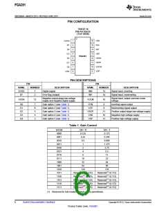
PIN CONFIGURATION
TSSOP-16
PW PACKAGE
(TOP VIEW)
1
2
3
4
5
6
7
8
16
VSN
DVDD
EF
15 INN
14 INP
13 VSP
G4
G3
PGA281
12
G2
VSON
G1
11 VSOP
10 VOCM
G0
VON
9
VOP
PIN DESCRIPTIONS
PIN
PIN
NAME
DVDD
EF
NUMBER
DESCRIPTION
Digital supply
NAME
INN
NUMBER
DESCRIPTION
Signal input, inverting
Signal input, noninverting
1
2
15
14
Error flag (output)
INP
Negative output-stage low-voltage
supply and negative digital supply
Signal input, output common-mode
voltage
VSON
12
VOCM
10
G0
G1
G2
G3
G4
7
6
5
4
3
Gain option 1 (see Table 1)
Gain option 2 (see Table 1)
Gain option 3 (see Table 1)
Gain option 4 (see Table 1)
Gain option 5 (see Table 1)
VON
VOP
VSOP
VSN
8
Inverting signal output
9
Noninverting signal output
11
16
13
Positive output-stage low-voltage supply
Negative high-voltage supply
Positive high-voltage supply
VSP
Table 1. Gain Control
G3:G0
0000
0001
0010
0011
0100
0101
0110
0111
1000
1001
1010
1011
1100
1101
1110
1111
G4 = 0
G4 = 1
0.172
0.344
0.688
1.375
2.75
5.5
0.125
0.25
0.5
1
2
4
8
11
16
22
32
44
64
88
128
176
Reserved(1) (0.125)
Reserved(1) (0.125)
Reserved(1) (0.125)
Reserved(1) (0.125)
Reserved(1) (0.125)
Reserved(1) (0.172)
Reserved(1) (0.172)
Reserved(1) (0.172)
Reserved(1) (0.172)
Reserved(1) (0.172)
(1) Reserved for test-modes. Default gain in parenthesis.
6
Submit Documentation Feedback
Copyright © 2013, Texas Instruments Incorporated
Product Folder Links: PGA281

 TI [ TEXAS INSTRUMENTS ]