PGA281
SBOS664A –MARCH 2013–REVISED JUNE 2013
www.ti.com
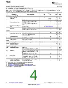
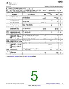
ELECTRICAL CHARACTERISTICS (continued)
At TA = +25°C, VSP = +15 V, VSN = –15 V, VSON = 0 V, VSOP = 5 V, DVDD = +3 V, RL = 2.5 kΩ to VSOP / 2 = VOCM,
G = 1 V/V, VCM = 0 V, and differential output, unless otherwise noted.
PGA281
PARAMETER
GAIN (Output Swing = ±4.5 V(6)
Range of input gain
TEST CONDITIONS
MIN
TYP
MAX
UNIT
)
⅛
128
V/V
V/V
Output gain
1 or 1⅜
All gains
±0.03%
±0.15%
±2
TA = –40°C to +105°C, no load, all gains
-0.5
-1
ppm/°C
ppm/°C
(8)
Gain error, all binary steps
except gain = 128 V/V(7)
TA = –40°C to +105°C, no load, gain = 128
V/V(7)(8)
±3
Gain step matching(9) (gain to
gain)
No load, all gains
See Typical Characteristics
No load, all gains(10)
No load, all gains, TA = –40°C to +105°C(7)
1.5
3
10
ppm
ppm
Nonlinearity
OUTPUT
VSOP = 5 V, load current 2 mA
TA = –40°C to +105°C
40
100
100
mV
mV
Voltage output swing from rail(9)
VSOP = 2.7 V, load current 1.5 mA
TA = –40°C to +105°C
Capacitive load drive
Short-circuit current
Output resistance
500
pF
mA
mΩ
ISC
To VSOP / 2, gain = 1.375 V/V
Both VOP and VON outputs
7
15
25
200
VOCM
IB(VOCM)
Voltage range for VOCM
Bias current into VOCM
VOCM input resistance
VSP – 2 V > VOCM, TA = –40°C to +105°C
(VSON) + 0.1
(VSOP) – 0.1
100
V
3
1
nA
GΩ
FREQUENCY RESPONSE
GBP
Gain bandwidth product(9)
Gain > 4 V/V
6
1
2
MHz
V/μs
V/μs
Gain = 1 V/V, 4-VPP output step, CL = 100 pF
Gain = 8 V/V, 4-VPP output step, CL = 100 pF
SR
Slew rate(9)
Gain = 128 V/V, 4-VPP output step, CL = 100
pF
1
V/μs
To 0.01%, gain = 8 V/V, VO = 8-VPP step
To 0.001%, gain = 8 V/V, VO = 8-VPP step
To 0.01%, gain = 128 V/V, VO = 8-VPP step
To 0.001%, gain = 128 V/V, VO = 8-VPP step
0.5 V over supply, gain = ⅛ V/V to 128 V/V
±5.5-VPP input, gain = 1 V/V
20
30
30
40
8
μs
μs
μs
μs
μs
μs
tS
Settling time(9)
Overload recovery, input(9)
Overload recovery, output(9)
6
(6) Gains smaller than ½ are measured with smaller output swing.
(7) Specified by design; not production tested.
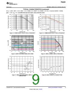
(8) See Figure 10 for typical gain error drift of various gain settings.
(9) See Application Information section and Typical Characteristic graphs.
(10) Only gain = 1 is production tested.
4
Submit Documentation Feedback
Copyright © 2013, Texas Instruments Incorporated
Product Folder Links: PGA281

 TI [ TEXAS INSTRUMENTS ]