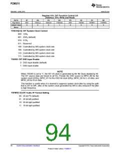
PCM9211
SBAS495 –JUNE 2010
www.ti.com
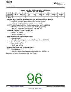
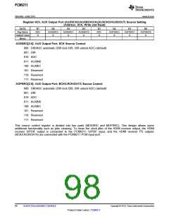
Register 6Ch, AUX Output Port (AUXSCKO/AUXBCKO/AUXLRCKO/AUXDOUT) Source Setting
(Address: 6Ch, Write and Read)
DATA
Reg Name
Default Value
Memo
B7
RSV
0
B6
AOSSRC2
0
B5
AOSSRC1
0
B4
AOSSRC0
0
B3
RSV
0
B2
AOPSRC2
0
B1
AOPSRC1
0
B0
AOPSRC0
0
AOSSRC[2:0]: AUX Output Port, SCK Source Control
000: DIR/ADC automatic (DIR lock:DIR, DIR unlock:ADC) (default)
001: DIR
010: ADC
011: AUXIN0
100: AUXIN1
101: Reserved
110: Reserved
111: Reserved
AOPSRC[2:0]: AUX Output Port, BCK/LRCK/DATA Source Control
000: DIR/ADC automatic (DIR lock:DIR, DIR unlock:ADC) (default)
001: DIR
010: ADC
011: AUXIN0
100: AUXIN1
101: Reserved
110: Reserved
111: Reserved
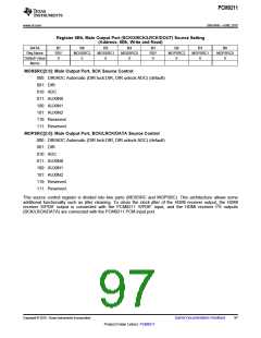
This source control register is divided into two parts (MOSSRC and MOPSRC). This design allows some
additional functionality such as jitter cleaning. To clean the clock jitter of the HDMI receiver output, the HDMI
receiver S/PDIF output is connected to the PCM9211 S/PDIF input, and the HDMI receiver I2S outputs
(BCK/LRCK/DATA) are connected with the PCM9211 PCM input port.
98
Submit Documentation Feedback
Copyright © 2010, Texas Instruments Incorporated
Product Folder Link(s): PCM9211

 TI [ TEXAS INSTRUMENTS ]