PCM9211
SBAS495 –JUNE 2010
www.ti.com
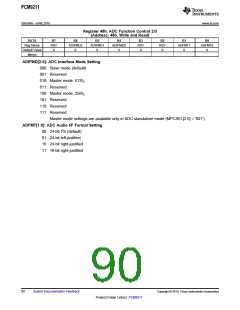
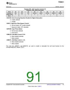
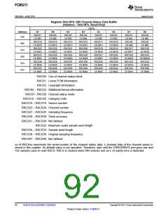
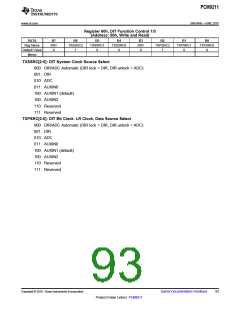
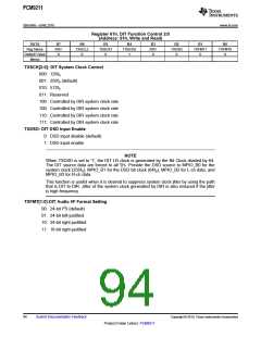
Register 61h, DIT Function Control 2/3
(Address: 61h, Write and Read)
DATA
Reg Name
Default Value
Memo
B7
RSV
0
B6
TXSCL2
0
B5
TXSCK1
0
B4
TXSCK0
1
B3
RSV
0
B2
TXDSD
0
B1
TXFMT1
0
B0
TXFMT0
0
TXSCK[2:0]: DIT System Clock Control
000: 128fS
001: 256fS (default)
010: 512fS
011: Reserved
100: Controlled by DIR system clock rate
100: Controlled by DIR system clock rate
110: Controlled by DIR system clock rate
111: Controlled by DIR system clock rate
TXDSD: DIT DSD Input Enable
0: DSD input disable (default)
1: DSD input enable
NOTE
When TXDSD is set to '1', the DIT LR clock is generated by the Bit Clock divided by 64.
The DIT source data are forced to all '0's. Provide the DSD source to MPIO_B0 for the
system clock (256fS), MPIO_B1 for the DSD bit clock (64fS), MPIO_B2 for L-ch data, and
MPIO_B3 for R-ch data.
This function is useful when it is desired to suppress system clock jitter by using the path
that is DIT to DIR. Jitter of the system clock generated by DIR is also reduced if the jitter
is high frequency.
TXFMT[1:0]:DIT Audio I/F Format Setting
00: 24-bit I2S (default)
01: 24-bit left-justified
10: 24-bit right-justified
11: 16-bit right-justified
94
Submit Documentation Feedback
Copyright © 2010, Texas Instruments Incorporated
Product Folder Link(s): PCM9211

 TI [ TEXAS INSTRUMENTS ]