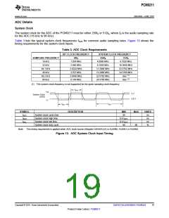
PCM9211
www.ti.com
SBAS495 –JUNE 2010
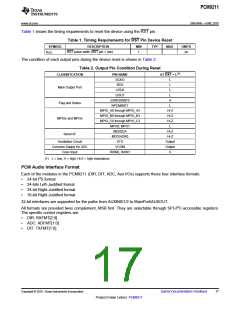
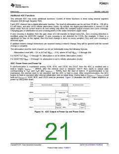
Table 1 shows the timing requirements to reset the device using the RST pin.
Table 1. Timing Requirements for RST Pin Device Reset
SYMBOL
tRSTL
DESCRIPTION
MIN
TYP
MAX
UNITS
µs
RST pulse width (RST pin = low)
1
The condition of each output pins during the device reset is shown in Table 2.
Table 2. Output Pin Condition During Reset
CLASSIFICATION
PIN NAME
SCKO
AT RST = L(1)
L
L
BCK
Main Output Port
LRCK
L
DOUT
L
ERROR/INT0
NPCM/INT1
H
Flag and Status
MPIOs and MPOs
Serial I/F
L
MPIO_A0 through MPIO_A3
MPIO_B0 through MPIO_B3
MPIO_C0 through MPIO_C3
MPO0, MPO1
MDI/SDA
Hi-Z
Hi-Z
Hi-Z
L
Hi-Z
Hi-Z
Output
Output
H
MDO/ADR0
Oscillation Circuit
Common Supply for ADC
Coax Input
XTO
VCOM
RXIN0, RXIN1
(1) L = low, H = high, Hi-Z = high impedance.
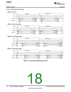
PCM Audio Interface Format
Each of the modules in the PCM9211 (DIR, DIT, ADC, Aux I/Os) supports these four interface formats:
•
•
•
•
24-bit I2S format
24-bits Left-Justified format
24-bit Right-Justified format
16-bit Right-Justified format
32-bit interfaces are supported for the paths from AUXIN0/1/2 to MainPort/AUXOUT.
All formats are provided twos complement, MSB first. They are selectable through SPI-/I2C-accessible registers.
The specific control registers are:
•
•
•
DIR: RXFMT[2:0]
ADC: ADFMT[1:0]
DIT: TXFMT[1:0]
Copyright © 2010, Texas Instruments Incorporated
Submit Documentation Feedback
17
Product Folder Link(s): PCM9211

 TI [ TEXAS INSTRUMENTS ]