10.4.2 Driver
PARAMETER
Differential output voltage
TEST CONDITION
MIN
MAX
UNIT
mV
mA
mA
mA
mV
V
56 Ω,
See Figure 10−1
172
265
OD
†
†
1.05
I
I
I
Driver difference current, TPA+, TPA−, TPB+, TPB−
Common-mode speed signaling current, TPB+, TPB−
Common-mode speed signaling current, TPB+, TPB−
Off state differential voltage
Drivers enabled, speed signaling off
S200 speed signaling enabled
S400 speed signaling enabled
−1.05
DIFF
‡
‡
−2.53
−4.84
SP200
SP400
‡
‡
−12.4
−8.10
V
OFF
Drivers disabled,
See Figure 10−1
20
†
‡
Limits defined as algebraic sum of TPA+ and TPA− driver currents. Limits also apply to TPB+ and TPB− algebraic sum of driver currents.
Limits defined as absolute limit of each of TPB+ and TPB− driver currents.
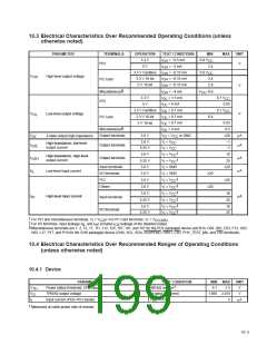
TPAx+
TPBx+
56 Ω
TPAx−
TPBx−
Figure 10−1. Test Load Diagram
10.4.3 Receiver
PARAMETER
TEST CONDITION
Drivers disabled
MIN TYP
MAX
UNIT
kΩ
pF
4
7
Z
Z
Differential impedance
ID
4
20
kΩ
pF
Common-mode impedance
Drivers disabled
IC
24
30
V
V
V
V
V
V
Receiver input threshold voltage
Drivers disabled
Drivers disabled
Drivers disabled
Drivers disabled
−30
0.6
mV
V
TH−R
Cable bias detect threshold, TPBx cable inputs
Positive arbitration comparator threshold voltage
Negative arbitration comparator threshold voltage
Speed signal threshold
1.0
TH−CB
+
−
89
168
−89
131
396
mV
mV
mV
mV
TH
TH
−168
49
TPBIAS−TPA common mode
voltage, drivers disabled
TH−SP200
TH−SP400
Speed signal threshold
314
10.5 PCI Clock/Reset Timing Requirements Over Recommended Ranges of Supply
Voltage and Operating Free-Air Temperature
ALTERNATE
SYMBOL
PARAMETER
TEST CONDITIONS
MIN
MAX
UNIT
t
t
t
Cycle time, PCLK
t
30
11
11
1
ns
ns
c
cyc
Pulse duration (width), PCLK high
Pulse duration (width), PCLK low
Slew rate, PCLK
t
high
w(H)
w(L)
t
ns
low
∆v/∆t
t , t
r f
4
V/ns
ms
ms
t
w
Pulse duration (width), GRST
Setup time, PCLK active at end of PRST
t
1
rst
t
su
t
100
rst-clk
10−4

 TI [ TEXAS INSTRUMENTS ]