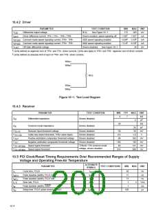
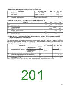
10.6 Switching Characteristics for PHY Port Interface
PARAMETER
TEST CONDITIONS
MIN
TYP
MAX
0.15
0.10
1.2
UNIT
ns
Jitter, transmit
Skew, transmit
Between TPA and TPB
Between TPA and TPB
ns
t
t
TP differential rise time, transmit
TP differential fall time, transmit
10% to 90%, at 1394 connector
90% to 10%, at 1394 connector
0.5
0.5
ns
r
1.2
ns
f
10.7 Operating, Timing, and Switching Characteristics of XI
PARAMETER
MIN
TYP
MAX
UNIT
V
DD
V
IH
V
IL
3.0
3.3
3.6 V (PLLV
)
CC
High-level input voltage
Low-level input voltage
Input clock frequency
Input clock frequency tolerance
Input slew rate
0.63V
CC
V
0.33V
V
CC
24.576
MHz
PPM
V/ns
<100
4
0.2
Input clock duty cycle
40%
60%
10.8 PCI Timing Requirements Over Recommended Ranges of Supply Voltage and
Operating Free-Air Temperature
This data manual uses the following conventions to describe time ( t ) intervals. The format is t , where subscript A
A
indicates the type of dynamic parameter being represented. One of the following is used: t = propagation delay time,
pd
t (t , t ) = delay time, t = setup time, and t = hold time.
d
en dis
su
h
ALTERNATE
SYMBOL
PARAMETER
TEST CONDITIONS
MIN
MAX
UNIT
PCLK-to-shared signal
valid delay time
t
11
val
inv
C
= 50 pF,
L
t
Propagation delay time, See Note 4
ns
pd
See Note 4
PCLK-to-shared signal
invalid delay time
t
2
2
t
t
t
t
Enable time, high impedance-to-active delay time from PCLK
Disable time, active-to-high impedance delay time from PCLK
Setup time before PCLK valid
t
ns
ns
ns
ns
en
dis
su
h
on
t
28
off
t
7
0
su
Hold time after PCLK high
t
h
NOTE 4: PCI shared signals are AD31−AD0, C/BE3−C/BE0, FRAME, TRDY, IRDY, STOP, IDSEL, DEVSEL, and PAR.
10−5

 TI [ TEXAS INSTRUMENTS ]