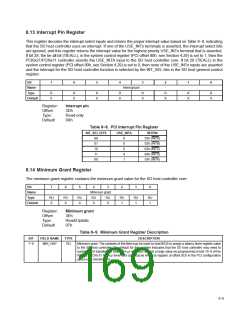
8.13 Interrupt Pin Register
This register decodes the interrupt select inputs and returns the proper interrupt value based on Table 8−8, indicating
that the SD host controller uses an interrupt. If one of the USE_INTx terminals is asserted, the interrupt select bits
are ignored, and this register returns the interrupt value for the highest priority USE_INTx terminal that is asserted.
If bit 28, the tie-all bit (TIEALL), in the system control register (PCI offset 80h, see Section 4.29) is set to 1, then the
PCI6x21/PCI6x11 controller asserts the USE_INTA input to the SD host controller core. If bit 28 (TIEALL) in the
system control register (PCI offset 80h, see Section 4.29) is set to 0, then none of the USE_INTx inputs are asserted
and the interrupt for the SD host controller function is selected by the INT_SEL bits in the SD host general control
register.
Bit
7
6
5
4
3
2
1
0
Name
Type
Default
Interrupt pin
R
0
R
0
R
0
R
0
R
0
R
X
R
X
R
X
Register:
Offset:
Type:
Interrupt pin
3Dh
Read-only
0Xh
Default:
Table 8−8. PCI Interrupt Pin Register
INT_SEL BITS
USE_INTA
INTPIN
00
01
10
11
0
0
0
0
1
01h (INTA)
02h (INTB)
03h (INTC)
04h (INTD)
01h (INTA)
XX
8.14 Minimum Grant Register
The minimum grant register contains the minimum grant value for the SD host controller core.
Bit
7
6
5
4
3
2
1
0
Name
Type
Default
Minimum grant
RU
0
RU
0
RU
0
RU
0
RU
0
RU
1
RU
1
RU
1
Register:
Offset:
Type:
Minimum grant
3Eh
Read/Update
07h
Default:
Table 8−9. Minimum Grant Register Description
BIT
FIELD NAME
TYPE
DESCRIPTION
7−0
MIN_GNT
RU
Minimum grant. The contents of this field may be used by host BIOS to assign a latency timer register value
to the SD host controller. The default for this register indicates that the SD host controller may need to
sustain burst transfers for nearly 64 µs and thus request a large value be programmed in bits 15−8 of the
PCI6x21/PCI6x11 latency timer and class cache line size register at offset 0Ch in the PCI configuration
space (see Section 8.6).
8−9

 TI [ TEXAS INSTRUMENTS ]