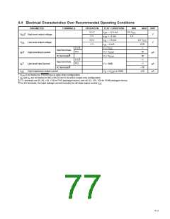
6.4 Electrical Characteristics Over Recommended Operating Conditions
PARAMETER
TERMINALS
OPERATION
3.3 V
TEST CONDITIONS
MIN
0.9 V
MAX
UNIT
I
I
I
I
= –0.5 mA
CC
2.4
OH
†
V
V
High-level output voltage
OH
5 V
= –2 mA
= 1.5 mA
= 6 mA
OH
OL
OL
3.3 V
0.1 V
CC
0.55
Low-level output voltage
High-level input current
V
OL
V
5 V
§
§
TTL
V = V
I
1
CC
Input terminals
‡
PCI
V = V
I
10
I
IH
CCP
µA
¶
I/O terminals
V = V
I
10
–1
CCP
TTL
PCI
Input terminals
‡
–1
I
I
Low-level input current
V = GND
µA
µA
IL
I
¶
–10
±10
I/O terminals
High-impedance output current
V
O
= V
or GND
CCP
OZ
†
‡
§
¶
V
is not tested on PSERR due to open-drain configuration.
and I are not tested on NO_HSLED dur to its active ourput-only configuration.
OH
I
IH
IL
TTL terminals are 55, 69, 132, 174 for PGF-packaged device; and 49, 63, 120, 159 for PCM-packaged device.
For I/O terminals, the input leakage current includes the off-state output current I
.
OZ
6–3

 TI [ TEXAS INSTRUMENTS ]