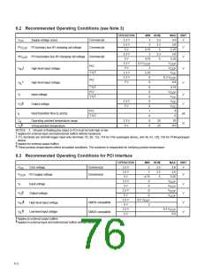
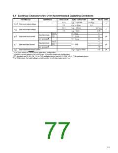
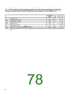
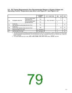
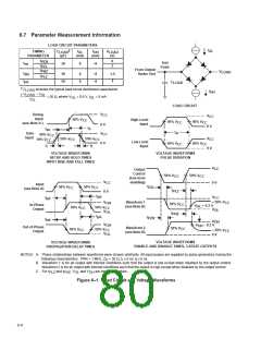
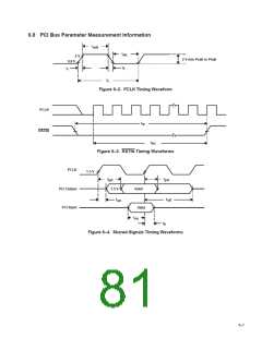
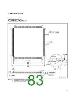
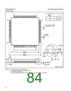
6.7 Parameter Measurement Information
LOAD CIRCUIT PARAMETERS
†
I
OL
TIMING
C
I
I
V
LOAD
(pF)
OL
OH
LOAD
(V)
PARAMETER
(mA)
(mA)
t
0
3
PZH
Test
Point
t
50
8
–8
en
t
t
t
PZL
PHZ
PLZ
From Output
Under Test
V
LOAD
t
t
50
50
8
8
–8
–8
1.5
‡
dis
pd
C
LOAD
†
‡
C
V
includes the typical load-circuit distributed capacitance.
LOAD
LOAD
I
OH
– V
OL
= 50 Ω, where V
= 0.6 V, I
= 8 mA
OL
OL
I
OL
LOAD CIRCUIT
V
Timing
Input
(see Note A )
CC
V
CC
50% V
High-Level
Input
CC
50% V
50% V
CC
CC
0 V
0 V
t
h
t
su
t
w
Data
Input
V
CC
90% V
CC
V
CC
50% V
50% V
10% V
CC
CC
CC
t
Low-Level
Input
0 V
50% V
50% V
CC
CC
0 V
t
f
r
VOLTAGE WAVEFORMS
SETUP AND HOLD TIMES
VOLTAGE WAVEFORMS
PULSE DURATION
INPUT RISE AND FALL TIMES
V
CC
Output
Control
(low-level
enabling)
50% V
50% V
CC
CC
V
0 V
CC
Input
(see Note A)
t
50% V
50% V
CC
PZL
CC
t
PLZ
0 V
t
pd
V
t
CC
pd
≈ 50% V
V
Waveform 1
(see Note B)
CC
CC
OH
50% V
CC
In-Phase
Output
V
+ 0.3 V
OL
50% V
50% V
CC
CC
V
OL
V
OL
t
PHZ
t
pd
t
PZH
t
pd
V
OH
V
OH
V
– 0.3 V
OH
Out-of-Phase
Output
Waveform 2
(see Note B)
50% V
CC
50% V
50% V
CC
CC
≈ 50% V
0 V
V
OL
VOLTAGE WAVEFORMS
ENABLE AND DISABLE TIMES, 3-STATE OUTPUTS
VOLTAGE WAVEFORMS
PROPAGATION DELAY TIMES
NOTES: A. Phase relationships between waveforms were chosen arbitrarily. All input pulses are supplied by pulse generators having the
following characteristics: PRR = 1 MHz, Z = 50 Ω, t ≤ 6 ns, t ≤ 6 ns.
O
r
f
B. Waveform 1 is for an output with internal conditions such that the output is low except when disabled by the output control.
Waveform 2 is for an output with internal conditions such that the output is high except when disabled by the output control.
C. For t
and t
, V
PHZ OL
and V
are measured values.
OH
PLZ
Figure 6–1. Load Circuit and Voltage Waveforms
6–6

 TI [ TEXAS INSTRUMENTS ]