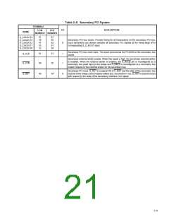
Table 2–9. Secondary PCI Address and Data
TERMINAL
PCM
I/O
DESCRIPTION
PGF
NAME
NUMBER NUMBER
36
35
33
32
31
29
28
26
24
22
21
20
18
17
16
14
156
155
153
152
150
149
148
146
144
142
141
140
138
137
136
134
38
37
35
34
33
31
30
28
26
24
23
22
20
19
18
16
170
169
167
166
164
163
162
160
158
156
155
154
152
151
150
148
S_AD31
S_AD30
S_AD29
S_AD28
S_AD27
S_AD26
S_AD25
S_AD24
S_AD23
S_AD22
S_AD21
S_AD20
S_AD19
S_AD18
S_AD17
S_AD16
S_AD15
S_AD14
S_AD13
S_AD12
S_AD11
S_AD10
S_AD9
Secondary address/data bus. These signals make up the multiplexed PCI address and data
bus on the secondary interface. During the address phase of a secondary bus PCI cycle,
S_AD31–S_AD0 contain a 32-bit address or other destination information. During the data
phase, S_AD31–S_AD0 contain data.
I/O
S_AD8
S_AD7
S_AD6
S_AD5
S_AD4
S_AD3
S_AD2
S_AD1
S_AD0
Secondary bus commands and byte enables. These signals are multiplexed on the same PCI
terminals.During the address phase of a secondary bus cycle, S_C/BE3–S_C/BE0definethe
buscommand. Duringthedataphase, this4-bitbusisusedasbyteenables. Thebyteenables
determinewhich byte paths of the full 32-bit data bus carry meaningful data. S_C/BE0 applies
to byte 0 (S_AD7–S_AD0), S_C/BE1 applies to byte 1 (S_AD15–S_AD8), S_C/BE2 applies
to byte 2 (S_AD23–S_AD16), and S_C/BE3 applies to byte 3 (S_AD31–S_AD24).
S_C/BE3
S_C/BE2
S_C/BE1
S_C/BE0
25
13
158
145
27
15
172
159
I/O
2–10

 TI [ TEXAS INSTRUMENTS ]