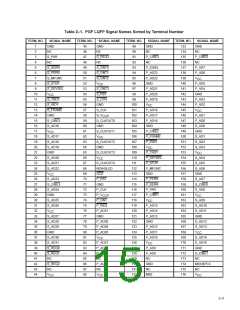
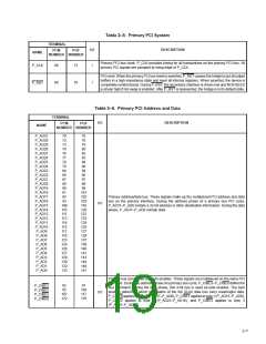
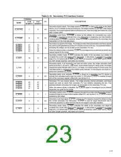
Table 2–5. Primary PCI System
TERMINAL
PCM
I/O
DESCRIPTION
PGF
NAME
NUMBER NUMBER
Primary PCI bus clock. P_CLK provides timing for all transactions on the primary PCI bus. All
primary PCI signals are sampled at rising edge of P_CLK.
P_CLK
66
64
72
70
I
PCI reset. When the primary PCI bus reset is asserted, P_RST causes the bridge to put all output
buffers in a high-impedance state and reset all internal registers. When asserted, the device is
completely nonfunctional. During P_RST, the secondary interface is driven low and NO/HSLED
is driven high if hot-swap is enabled. After P_RST is deasserted, the bridge is in its default state.
I
P_RST
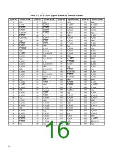
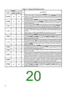
Table 2–6. Primary PCI Address and Data
TERMINAL
PCM
I/O
DESCRIPTION
PGF
NAME
NUMBER NUMBER
P_AD31
P_AD30
P_AD29
P_AD28
P_AD27
P_AD26
P_AD25
P_AD24
P_AD23
P_AD22
P_AD21
P_AD20
P_AD19
P_AD18
P_AD17
P_AD16
P_AD15
P_AD14
P_AD13
P_AD12
P_AD11
P_AD10
P_AD9
70
72
73
74
76
77
78
79
84
85
87
88
89
91
92
93
109
110
111
113
114
115
117
118
123
124
126
127
129
130
132
133
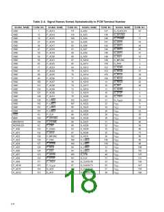
76
78
79
80
82
83
84
86
94
95
97
98
99
101
102
103
119
120
121
123
124
125
127
128
137
138
140
141
143
144
146
147
Primary address/data bus. These signals make up the multiplexed PCI address and data
bus on the primary interface. During the address phase of a primary bus PCI cycle,
P_AD31–P_AD0 contain a 32-bit address or other destination information. During the data
phase, P_AD31–P_AD0 contain data.
I/O
P_AD8
P_AD7
P_AD6
P_AD5
P_AD4
P_AD3
P_AD2
P_AD1
P_AD0
Primary bus commands and byte enables. These signals are multiplexed on the same PCI
terminals. During the address phase of a primary bus cycle, P_C/BE3–P_C/BE0 define the
bus command. During the data phase, this 4-bit bus is used as byte enables. The byte
enables determine which byte paths of the full 32-bit data bus carry meaningful data.
P_C/BE0applies to byte 0 (P_AD7–P_AD0), P_C/BE1 applies to byte 1 (P_AD15–P_AD8),
P_C/BE2 applies to byte 2 (P_AD23–P_AD16), and P_C/BE3 applies to byte 3
(P_AD31–P_AD24).
82
95
107
122
91
P_C/BE3
P_C/BE2
P_C/BE1
P_C/BE0
105
117
135
I/O
2–7

 TI [ TEXAS INSTRUMENTS ]