3 Feature/Protocol Descriptions
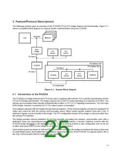
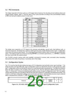
The following sections give an overview of the PCI2250 PCI-to-PCI bridge features and functionality. Figure 3–1
shows a simplified block diagram of a typical system implementation using the PCI2250.
Host Bus
Memory
CPU
Host
PCI
PCI
Bridge
Device
Device
PCI Bus 0
PCI Option Card
PCI Option Card
PCI2250
PCI Bus 2
PCI Bus 1
PCI
Device
PCI
Device
(Option)
PCI2250
PCI Option Slot
Figure 3–1. System Block Diagram
3.1 Introduction to the PCI2250
The PCI2250 is a bridge between two PCI buses and is compliant with both the PCI Local Bus Specification and the
PCI-to-PCI Bridge Specification. The bridge supports two 32-bit PCI buses operating at a maximum of 33 MHz. The
primary and secondary buses operate independently in either a 3.3-V or 5-V signaling environment. The core logic
of the bridge, however, is powered at 3.3 V to reduce power consumption.
Host software interacts with the bridge through internal registers. These internal registers provide the standard PCI
status and control for both the primary and secondary buses. Many vendor-specific features that exist in the TI
extension register set are included in the bridge. The PCI configuration header of the bridge is only accessible from
the primary PCI interface.
The bridge provides internal arbitration for the four possible secondary bus masters, and provides each with a
dedicated active low request/grant pair (REQ/GNT). The arbiter features a two-tier rotational scheme with the
PCI2250 bridge defaulting to the highest priority tier. The bus parking scheme is also configurable and can be set
to either park grant (GNT) on the bridge or on the last mastering device.
Upon system power up, power-on self-test (POST) software configures the bridge according to the devices that exist
on subordinate buses, and enables the performance-enhancing features of the PCI2250. In a typical system, this is
the only communication with the bridge internal register set.
3–1

 TI [ TEXAS INSTRUMENTS ]