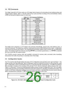
3.2 PCI Commands
The bridge responds to PCI bus cycles as a PCI target device based on the decoding of each address phase and
internal register settings. Table 3–1 lists the valid PCI bus cycles and their encoding on the command/byte enables
(C/BE) bus during the address phase of a bus cycle.
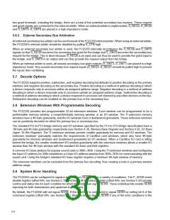
Table 3–1. PCI Command Definition
COMMAND
Interrupt acknowledge
Special cycle
C/BE3–C/BE0
0000
0001
0010
0011
I/O read
I/O write
0100
0101
0110
Reserved
Reserved
Memory read
0111
Memory write
1000
1001
1010
1011
Reserved
Reserved
Configuration read
Configuration write
Memory read multiple
Dual address cycle
Memory read line
Memory write and invalidate
1100
1101
1110
1111
The bridge never responds as a PCI target to the interrupt acknowledge, special cycle, dual address cycle, or
reserved commands. The bridge does, however, initiate special cycles on both interfaces when a type 1 configuration
cycle issues the special cycle request. The remaining PCI commands address either memory, I/O, or configuration
space. The bridge accepts PCI cycles by asserting DEVSEL as a medium-speed device, i.e., DEVSEL is asserted
two clock cycles after the address phase.
The PCI2250 converts memory write and invalidate commands to memory write commands when forwarding
transactions from either the primary or secondary side of the bridge.
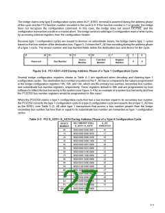
3.3 Configuration Cycles
The PCI Local Bus Specification defines two types of PCI configuration read and write cycles: type 0 and type 1. The
bridge decodes each type differently. Type 0 configuration cycles are intended for devices on the primary bus, while
type 1 configuration cycles are intended for devices on some hierarchically subordinate bus. The difference between
these two types of cycles is the encoding of the primary PCI (P_AD) bus during the address phase of the cycle.
Figure 3–2 shows the P_AD bus encoding during the address phase of a type 0 configuration cycle. The 6-bit register
number field represents an 8-bit address with the two lower bits masked to 0, indicating a doubleword boundary. This
results in a 256-byte configuration address space per function per device. Individual byte accesses may be selected
within a doubleword by using the P_C/BE signals during the data phase of the cycle.
31
11 10
8
7
2
1
0
0
Function
Number
Register
Number
Reserved
0
Figure 3–2. PCI AD31–AD0 During Address Phase of a Type 0 Configuration Cycle
3–2

 TI [ TEXAS INSTRUMENTS ]