P82B715
I2C BUS EXTENDER
www.ti.com
SCPS145A–DECEMBER 2007–REVISED FEBRUARY 2008
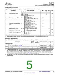
Electrical Characteristics
VCC = 5 V, TA = 25°C, voltages are specified with respect to GND (unless otherwise specified)
PARAMETER
TEST CONDITIONS
MIN
TYP
14
MAX UNIT
Sx = Sy = VCC
VCC = 12 V
15
ICC
Quiescent supply current
mA
Both I2C inputs low,
Both buffered outputs sinking 30 mA
22
VCC > 3 V,
VSx, VSy (low) = 0.4 V,
IIOS
Output sink current on I2C bus
Sx, Sy
2.6
mA
VLx, VLy (low) on buffered bus = 0.3 V,
ILx, ILy = –3 mA(1)
VLx, VLy (low) = 0.4 V,
30
24
VSx, VSy (low) on I2C bus = 0.3 V
3 V < VCC < 4.5 V,
Output sink current on buffered
bus
VLx, VLy (low) = 0.4 V to 1.5 V,
IIOL
Lx, Ly
mA
ISx, ISy sinking on I2C bus < –4 mA
3 V < VCC < 4.5 V,
VLx, VLy (low) = 1.5 V to VCC
,
24
ISx, ISy sinking on I2C bus = –7 mA
Input current from I2C bus
Sx, Sy ILx, ILy sink on buffered bus = 30 mA
–3.2
mA
–3
VCC > 3 V,
Input current from buffered bus(1)
ISx, ISy sink on I2C bus = 3 mA(1)
II
Lx, Ly
VCC = 3 V to 12 V,
VLx, VLy = VCC
VSx, VSy = VCC
Leakage current on buffered bus
Input/output impedance
,
200
13
µA
Zin/Zout
VSx < VLx, Buffer is active
8
10
(1) Buffer is passive in this test. The Sx/Sy sink current flows via an internal resistor to the driver connected at the Lx/Ly I/O.
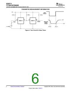
Switching Characteristics
VCC = 5 V, TA = 25°C, no capacitive loads, voltages are specified with respect to GND (unless otherwise specified)
FROM
(INPUT)
TO
(OUTPUT)
PARAMETER
TEST CONDITIONS
TYP UNIT
Buffer Delay Times
Delay time to VLx voltage crossing VCC/2 for input drive
current step ISx at Sx(1) (see Figure 2)
ISx
ISy
VLx
VLy
RLx pullup = 270 Ω
RLx pullup = 4700 Ω
250
0
ns
ns
trise/fall
Buffer delay time, switching edges between VLx input and
VSx output(2)
VLx
VLy
VSx
VSy
(1) A conventional input-output delay is not observed in the Sx/Lx voltage waveforms, because the input and output pins are internally tied
with a 30-Ω resistor so they show equal logic voltage levels to within 100 mV. When connected in an I2C system, an Sx/Sy input pin
cannot rise/fall until the buffered bus load at the output pin has been driven by the internal amplifier. This test measures the bus
propagation delay caused to falling or rising voltages at the Lx/Ly output (as well as the Sx/Sy input) by the amplifier’s response time.
The figure given is measured with a drive current as shown in Figure 2. Because this is a dynamic bus test in which a corresponding
bus driving IC has an output voltage well above 0.4 V, 6 mA is used instead of the static 3 mA.
(2) The signal path Lx to Sx and Ly to Sy is passive via the internal 30-Ω resistor. There is no amplifier involved and essentially no signal
propagation delay.
Copyright © 2007–2008, Texas Instruments Incorporated
Submit Documentation Feedback
5
Product Folder Link(s): P82B715

 TI [ TEXAS INSTRUMENTS ]