P82B715
I2C BUS EXTENDER
www.ti.com
SCPS145A–DECEMBER 2007–REVISED FEBRUARY 2008
APPLICATION INFORMATION
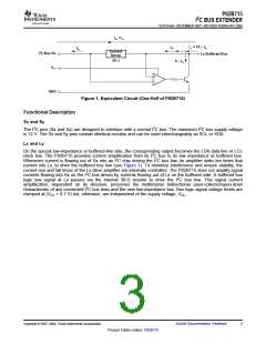
By using two (or more) P82B715 devices, a subsystem can be built that retains the interface characteristics of a
normal I2C device so that the subsystem may be included in, or added to, any I2C or related system.
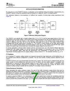
The subsystem features a low-impedance or buffered bus capable of driving large wiring capacitance (see
Figure 3).
VCC
P82B715
½
P82B715
½
LDA
LCL
SDA
SCL
SDA
SCL
I2C
Device
Long
Cable
½
½
Standard
I2C Bus
Special
Buffered
Bus
Special
Buffered
Bus
Standard
I2C Bus
Figure 3. Minimum Subsystem Diagram
The P82B715 can operate with a supply voltage from 3 V to 12.5 V, but the logic-signal levels at Sx/Lx are
independent of the supply voltage. They remain at the levels presented to the chip by the attached devices. The
maximum static I2C bus sink current, 3 mA, flowing in either direction in the internal current sense resistor,
causes a difference less than 100 mV in the bus logic low levels at Sx and Lx. This makes P82B715 fully
compatible with all logic signal drivers, including TTL. The P82B715 cannot modify the bus logic signal voltage
levels, but it contains internal diodes connected between Lx/Sx and VCC that conduct and limit the logic signal
swing if the applied logic levels would have exceeded the supply voltage by more than 0.7 V.
In normal applications, external pullup resistors pull the connected buses up to the desired voltage high level.
Usually this is the supply voltage, VCC, but for very low logic voltages, it is necessary to use a VCC of at least
3.3 V and preferably higher. Note that full performance over temperature is ensured only from 4.5 V.
Specification deratings apply when its supply voltage is reduced below 4.5 V. The absolute minimum VCC is 3 V.
I2C Systems
As in standard I2C systems, pullup resistors are required to provide the logic high levels on the buffered bus, as
the standard open-collector configuration is retained. The size and number of pullup resistors depends on the
system.
If P82B715 devices are to be permanently connected into a system, the circuit may be configured with only one
pullup resistor on the buffered bus and none on the I2C buses, but the system design is simplified, and
performance is improved by fitting separate pullups on each section of the bus. When a subsystem using
P82B715 may be optionally connected to an existing I2C system that already has a pullup, the effects of the
subsystem pullups acting in parallel with the existing I2C bus pullup must be considered.
Pullup Resistance Calculation
When calculating the pullup resistance values, the gain of the buffer introduces scaling factors that must be
applied to the system components. In practical systems, the pullup resistance value is calculated to meet the rise
time limit for I2C systems. As an approximation, this limit is satisfied in a 100-kHz system if the time constant of
the total system (product of the net resistance and net capacitance) is set to 1 µs or less.
In systems using the P82B715, it is convenient to set the total system time constant by considering each bus
node separately (i.e., the I2C nodes and the buffered bus node) and selecting a separate pullup resistor for each
node to provide time constants of less than 1 µs. If each node complies then the system requirement is also met.
Copyright © 2007–2008, Texas Instruments Incorporated
Submit Documentation Feedback
7
Product Folder Link(s): P82B715

 TI [ TEXAS INSTRUMENTS ]