P82B715
I2C BUS EXTENDER
www.ti.com
SCPS145A–DECEMBER 2007–REVISED FEBRUARY 2008
DESCRIPTION/ORDERING INFORMATION (CONTINUED)
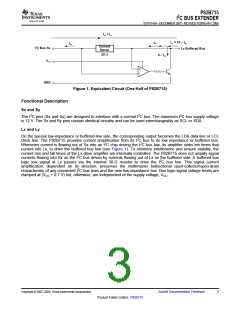
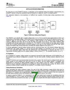
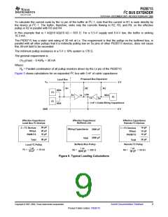
In general, the I2C bus capacitance limit of 400 pF restricts practical communication distances to a few meters.
One of the advantages of the P82B715 is that it can isolate bus capacitance such that the total loading (devices,
connectors, traces and wires) of the new bus or remote I2C nodes are not apparent to other I2C buses (or
nodes). This is achieved by using one P82B715 device at each end of a long cable. The pin Lx of one P82B715
device has to be connected to Lx of the second P82B715 (similarly for Ly). This allows the total system
capacitance load to be around 3000 pF. The P82B715 uses unidirectional analog current amplification to
increase the current sink capability of I2C chips by a factor of ten and to change the 400-pF I2C bus specification
limit into a 4-nF bus wiring capacitance limit. That means longer cables or lower-cost general-purpose wiring may
be used to connect two separate I2C-based systems, without worrying about the special voltage levels
associated with other I2C bus buffers.
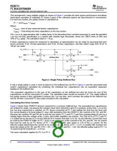
Multiple P82B715s can be connected together in a star or multipoint architecture by their Lx/Ly ports, without
limit, as long as the total capacitance of the system remains less than about 3000 pF (400 pF or less when
referenced to any Sx/Sy connection). In that arrangement, the master and/or slave devices are attached to the
Sx/Sy port of each P82B715. The P82B715 alone does not support voltage-level translation, but it simplifies the
application of low-cost transistors for this purpose. In normal use, the power-supply voltages at each end of the
low-impedance buffered bus line should be the same. If these differ by a significant amount, noise margin is
sacrificed.
Two or more Sx or Sy I/Os can be interconnected and are also fully compatible with bus buffers that use
voltage-level offsets (such as the PCA9515A) because it duplicates and transmits the offset voltage.
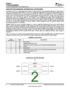
TERMINAL FUNCTIONS
D OR P
PACKAGE NO.
NAME
DESCRIPTION
1
2
3
4
5
6
7
8
NC
Lx
No connection
Buffered serial data bus or LDA
Serial data bus or SDA. Connect to VCC of I2C master through a pullup resistor.
Sx
GND
NC
Sy
Ground
No connection
Serial clock bus or SCL. Connect to VCC of I2C master through a pullup resistor.
Ly
Buffered serial clock bus or LCL
Supply voltage
VCC
FUNCTIONAL BLOCK DIAGRAM
VCC
P82B715
Buffer
Sx/SDA
Lx/LDA
Ly/LCL
Buffer
Sy/SCL
GND
2
Submit Documentation Feedback
Copyright © 2007–2008, Texas Instruments Incorporated
Product Folder Link(s): P82B715

 TI [ TEXAS INSTRUMENTS ]