P82B715
I2C BUS EXTENDER
www.ti.com
SCPS145A–DECEMBER 2007–REVISED FEBRUARY 2008
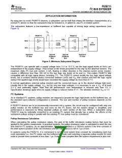
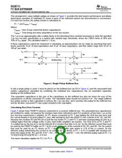
This arrangement, using multiple pullups as shown in Figure 4, provides the best system performance and allows
stand-alone operation of individual I2C buses if parts of the extended system are disconnected or reconnected.
For each bus section, the pullup resistor is calculated as:
R = 1 µs/(Cdevice + Cwiring
)
Where:
Cdevice = Sum of any connected device capacitances
Cwiring = Total wiring and stray capacitance on the bus section
The 1 µs is an approximation with a safety factor to the theoretical time constant necessary to meet the specified
1-µs bus rise-time specification in a system with variable logic thresholds, where the CMOS limits of 30% and
70% of VCC apply. The calculated value is 1.18 µs.
If these capacitances cannot be measured or calculated, an approximation can be made by assuming that each
device presents 10 pF of load capacitance and 10 pF of trace capacitance, and that cables range from 50 pF to
100 pF per meter.
VCC = 5 V
R3
R1
R2
SDA
SCL
SDA
SCL
Sx
Sy
Lx
Ly
Lx
Ly
Sx
Sy
I2C 1
I2C 2
Buffered Bus
VCC = 5 V
R4
SDA
SCL
Lx
Ly
Sx
Sy
I2C 3
Figure 4. Single Pullup Buffered Bus
If only a single pullup is used, it must be placed on the buffered bus (as R2 in Figure 4,) and the associated total
system capacitance calculated by combining the individual bus capacitances into an equivalent capacitive
loading on the buffered bus.
This equivalent capacitance is the sum of the capacitance on the buffered bus plus ten times the sum of the
capacitances on all the connected I2C nodes. The calculated value should not exceed 4 nF. The single buffered
bus pullup resistor is then calculated to achieve the 1-µs rise time, and it provides the pullup for the buffered bus
and for all other connected I2C bus nodes included in the calculation.
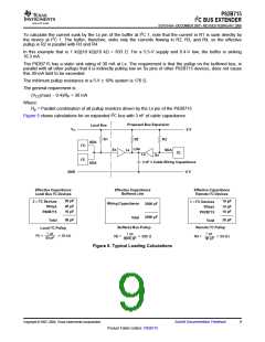
Calculating Bus Drive Currents
Figure 4 shows three P82B715 devices connected to a common buffered bus. The associated bus capacitances
are omitted for clarity, but assume the resistors have been selected to give R-C products of less than 1 µs so the
bus rise-time requirement is satisfied. An I2C device connected at I2C 1 and holding the SDA bus low must sink
the current flowing in its local pullup R1, plus, with assistance from the P82B715, the currents in R2, R3, and R4.
Because the resistors R3 and R4 act to pull the bus nodes I2C 2 and I2C 3 and their corresponding Sx pins to a
voltage higher than the voltage at the Lx pins, their buffer amplifiers are inactive. The SDA at Sx of I2C 2 and I2C
3 is pulled low by the low at Lx via the internal 30-Ω resistor that links Lx to Sx. So the effective current that must
be sunk by the P82B715 buffer on I2C 1 at its Lx pin is the sum of the currents in R2, R3, and R4. The Sx current
that must be sunk by an I2C device at I2C 1 due to the buffer gain action is 1/10 of the Lx current. So the
effective pullup determining the current to be sunk by an I2C device at I2C 1 is R1 in parallel with resistors ten
times the values of R2, R3, and R4. If R1 = R3 = R4 = 10 kΩ, and R2 = 1 kΩ, the effective pullup load at I2C 1 is
10 kΩ||10 kΩ||100 kΩ||100 kΩ = 4.55 kΩ.
The same calculation applies for I2C 2 or I2C 3.
8
Submit Documentation Feedback
Copyright © 2007–2008, Texas Instruments Incorporated
Product Folder Link(s): P82B715

 TI [ TEXAS INSTRUMENTS ]