P82B715
I2C BUS EXTENDER
www.ti.com
SCPS145A–DECEMBER 2007–REVISED FEBRUARY 2008
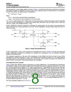
ISx = ILx
ILx = 10 ´ ISx
Lx Buffered Bus
ISx
ISx
I2C Bus Sx
Current
Sense
30 W
9 ´ ISx
VCC
+
–
GND
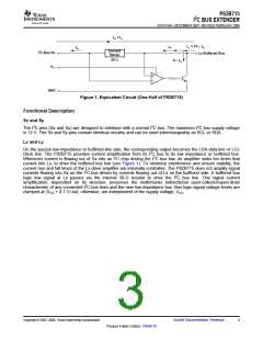
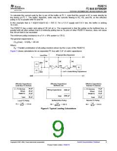
Figure 1. Equivalent Circuit (One-Half of P82B715)
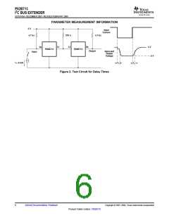
Functional Description
Sx and Sy
The I2C pins (Sx and Sy) are designed to interface with a normal I2C bus. The maximum I2C bus supply voltage
is 12 V. The Sx and Sy pins contain identical circuitry and can be used interchangeably as SCL or SDA.
Lx and Ly
On the special low-impedance or buffered-line side, the corresponding output becomes the LDA data line or LCL
clock line. The P82B715 provides current amplification from its I2C bus to its low impedance or buffered bus.
Whenever current is flowing out of Sx into an I2C chip driving the I2C bus low, its amplifier sinks ten times that
current into Lx, to drive the buffered bus low (see Figure 1). To minimize interference and ensure stability, the
current rise and fall times of the Lx drive amplifier are internally controlled. The P82B715 does not amplify signal
currents flowing into Sx on the I2C bus driven by currents flowing out of Lx on the buffered side. A buffered bus
logic low signal at Lx passes via the internal 30-Ω resistor to drive the I2C bus low. This signal current
amplification, dependent on its direction, preserves the multimaster bidirectional open-collector/open-drain
characteristic of any connected I2C bus lines and the new low-impedance bus. Bus logic-signal voltage levels are
clamped at (VCC + 0.7 V) but, otherwise, are independent of the supply voltage, VCC
.
Copyright © 2007–2008, Texas Instruments Incorporated
Submit Documentation Feedback
3
Product Folder Link(s): P82B715

 TI [ TEXAS INSTRUMENTS ]