ONET1131EC
ZHCSFG0 –SEPTEMBER 2016
www.ti.com.cn
UNIT
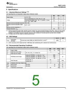
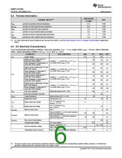
6.4 Thermal Information
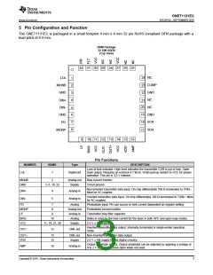
RSM (VQFN)
32 PINS
37.2
THERMAL METRIC(1)
RθJA
Junction-to-ambient thermal resistance
Junction-to-case (top) thermal resistance
Junction-to-board thermal resistance
°C/W
°C/W
°C/W
°C/W
°C/W
°C/W
RθJCtop
RθJB
30.1
7.8
ψJT
Junction-to-top characterization parameter
Junction-to-board characterization parameter
Junction-to-case (bottom) thermal resistance
0.4
ψJB
7.6
RθJCbot
2.4
(1) For more information about traditional and new thermal metrics, see the Semiconductor and IC Package Thermal Metrics application
report.
6.5 DC Electrical Characteristics
Over recommended operating conditions, open loop operation, VOUT = 2 VPP single-ended, I(BIAS) = 80 mA, unless otherwise
noted. Typical operating condition is at VCC = 2.5 V and TA = 25°C
PARAMETER
TEST CONDITIONS
MIN
TYP
MAX
UNIT
VCC
Supply voltage
2.37
2.5
2.63
V
Supply current in single-ended TX
mode with CDRs enabled
158
380
197
493
119
298
164
193
508
237
623
193
376
200
526
mA
mW
mA
mW
mA
mW
mA
TXMODE = 1, TXCDR_DIS = 0, TX VOUT = 2
VPP single-ended, I(BIAS) = 0 mA
Power dissipation in single-ended TX
mode with CDRs enabled
Supply current in differential TX mode
with CDRs enabled
TXMODE = 0, TXCDR_DIS = 0, TX VOUT = 2
VPP single-ended, I(BIAS) = 0 mA
Power dissipation in differential TX
mode with CDRs enabled
IVCC
Supply current in single-ended TX
mode with CDRs disabled
TXMODE = 1, TXCDR_DIS = 1, TX VOUT = 2
VPP single-ended, I(BIAS) = 0 mA
Power dissipation in single-ended TX
mode with CDRs disabled
Supply current in differential TX mode
with CDRs disabled
TXMODE = 0, TXCDR_DIS = 1, TX VOUT = 2
VPP single-ended, I(BIAS) = 0 mA;
Power dissipation in differential TX
mode with CDRs disabled
410
100
mW
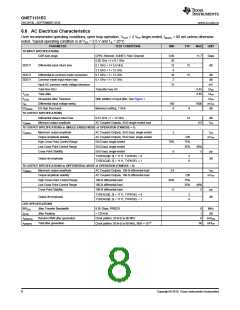
R(IN)
Data input resistance
Data input termination mismatch
Ooutput resistance
Differential between DIN+ / DIN–
Ω
5%
20
R(OUT)
Single-ended at OUT+ or OUT–
DIS pull up to VCC
60
Ω
Digital input current
–20
2.1
µA
LOL, FLT pull-up to VCC
,
VOH
Digital output high voltage
V
ISOURCE = 37.5 μA
LOL, FLT pull-up to VCC
ISINK = 350 μA
,
VOL
Digital output low voltage
Minimum bias current
0.4
5
V
(1)
I(BIAS-MIN)
See
mA
mA
Source. BIASPOL = 0, DAC set to maximum,
open and closed loop
145
95
150
100
I(BIAS-MAX)
Maximum bias current
Sink. BIASPOL = 1, DAC set to maximum,
open and closed loop
mA
I(BIAS-DIS)
Bias current during disable
Average power stability
100
µA
dB
V
APC loop enabled
±0.5
±3
Source. TXBIASPOL = 0
Sink. TXBIASPOL = 1
VCC - 0.45
Bias pin compliance voltage
Temperature sensor accuracy
0.45
V
With 1-point external mid-scale calibration
°C
(1) The bias current can be set below the specified minimum according to the corresponding register setting; however, in closed loop
operation settings below the specified value may trigger a fault.
6
Copyright © 2016, Texas Instruments Incorporated

 TI [ TEXAS INSTRUMENTS ]