ONET1131EC
ZHCSFG0 –SEPTEMBER 2016
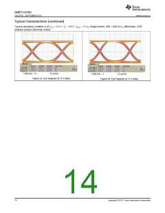
www.ti.com.cn
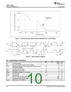
Figure 1. Input Sinusoidal Jitter Tolerance (INF-8077i Rev. 4.5 XFP MSA)
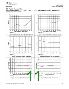
SDA
SCK
tBUFœ
tLOW
tf
tHDSTA
tr
tHIGH
P
S
S
P
tHDDAT
tSUDAT
tHDSTA
tSUSTA
tSUSTO
Figure 2. 2-Wire Interface Diagram
6.8 Timing Diagram Definitions
MIN
TYP
MAX
UNIT
kHz
µs
fSCK
SCK clock frequency
400
tBUF
Bus free time between START and STOP conditions
1.3
0.6
tHDSTA
Hold time after repeated START condition. After this period, the first
clock pulse is generated
µs
tLOW
tHIGH
tSUSTA
tHDDAT
tSUDAT
tR
Low period of the SCK clock
High period of the SCK clock
Setup time for a repeated START condition
Data HOLD time
1.3
0.6
0.6
0
µs
µs
µs
µs
ns
ns
ns
µs
Data setup time
100
Rise time of both SDA and SCK signals
Fall time of both SDA and SCK signals
Setup time for STOP condition
300
300
tF
tSUSTO
0.6
10
Copyright © 2016, Texas Instruments Incorporated

 TI [ TEXAS INSTRUMENTS ]