ONET1131EC
www.ti.com.cn
ZHCSFG0 –SEPTEMBER 2016
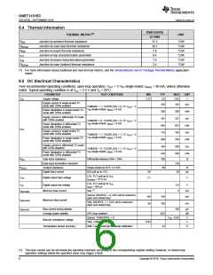
5 Pin Configuration and Function
The ONET1131EC is packaged in a small footprint 4 mm x 4 mm 32 pin RoHS compliant QFN package with a
lead pitch of 0.4 mm.
RSM Package
32 PIN VQFN
(Top View)
32 31 30 29 28 27 26 25
NC
24
23
LOL
MONB
GND
1
2
COMP
22 GND
3
4
NC
21
DIN+
DIN-
20 NC
5
6
GND
PD
19 GND
SCK
SDA
18
17
7
8
MONP
9
10 11 12 13 14 15 16
Pin Functions
NUMBER
LOL
NAME
Type
DESCRIPTION
Loss of lock indicator. High level indicates the transmitter CDR is out of lock. Open
drain output. Requires an external 4.7 kΩ to 10 kΩ pull-up resistor to VCC for proper
operation. This pin is 3.3 V tolerant.
1
Digital-out
MONB
GND
2
Analog-out
Supply
Bias current monitor.
Circuit ground.
3, 6, 19, 22
4
Non-inverted transmitter data input. On-chip differentially 100 Ω terminated to TXIN–.
Must be AC coupled.
DIN+
DIN–
Analog-in
Analog-in
Inverted transmitter data input. On-chip differentially 100 Ω terminated to TXIN+. Must
be AC coupled.
5
PD
7
Analog
Analog-out
Analog-in
Analog
Photodiode input. Pin can source or sink current dependent on register setting.
Photodiode current monitor.
MONP
LF
8
9
10
Transmitter loop filter capacitor.
BIAS
VCC
Sinks or sources the bias current for the laser in both APC and open loop modes.
2.5 V ± 5% supply.
11, 14, 27, 30
Supply
Inverted transmitter data output. Internally terminated in single-ended operation
mode.
OUT–
12
CML-out
OUT+
VDD
13
15
CML-out
Supply
Non-Inverted transmitter data output.
2.5 V ± 5% supply for the digital circuitry.
Output amplitude control. Output amplitude can be adjusted by applying a voltage of
0 to 2 V to this pin. Leave open when not used.
AMP
16
Analog-in
Copyright © 2016, Texas Instruments Incorporated
3

 TI [ TEXAS INSTRUMENTS ]