ONET1131EC
www.ti.com.cn
ZHCSFG0 –SEPTEMBER 2016
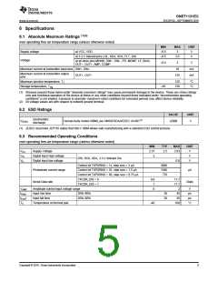
6 Specifications
6.1 Absolute Maximum Ratings
(1)(2)
over operating free-air temperature range (unless otherwise noted)
MIN
–0.5
–0.5
MAX
3
UNIT
V
Supply voltage
Voltage
at VCC, VDD
at 3.3-V tolerant pins LOL, SDA, SCK, FLT, DIS
3.6
V
at all other pins MONB, DIN+, DIN–, PD, MONP, LF, BIAS,
OUT–, OUT+, AMP, COMP
–0.5
3
V
Maximum current at transmitter input pins DIN+, DIN–
10
mA
mA
Maximum current at transmitter output
OUT+, OUT–
125
pins
Maximum junction temperature, TJ
Storage temperature, Tstg
125
150
°C
°C
–65
(1) Stresses beyond those listed under “absolute maximum ratings” may cause permanent damage to the device. These are stress ratings
only and functional operation of the device at these or any other conditions beyond those indicated under “recommended operating
conditions” is not implied. Exposure to absolute–maximum–rated conditions for extended periods may affect device reliability.
(2) All voltage values are with respect to network ground terminal.
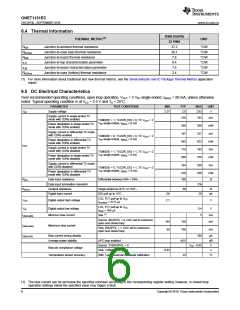
6.2 ESD Ratings
VALUE
UNIT
Electrostatic
discharge
V(ESD)
Human-body model (HBM), per ANSI/ESDA/JEDEC JS-001(1)
±2000
V
(1) JEDEC document JEP155 states that 500-V HBM allows safe manufacturing with a standard ESD control process.
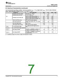
6.3 Recommended Operating Conditions
over operating free-air temperature range (unless otherwise noted)
MIN
2.37
2
TYP
MAX
UNIT
VCC
VIH
VIL
Supply Voltage
2.5
2.63
V
V
V
Digital input high voltage
Digital input low voltage
DIS, SCK, SDA, 3.3-V tolerant IOs
0.8
Control bit TXPDRNG = 1x, step size = 3 µA
Control bit TXPDRNG = 01, step size = 1.5 µA
Control bit TXPDRNG = 00, step size = 0.75 µA
TXCDR_DIS = 0
3080
1540
770
Photodiode current range
µA
9.8
1
11.7
11.7
2
Serial Data rate
Gbps
TXCDR_DIS = 1
VAMP
tR(IN)
Amplitude control input voltage range
0
V
Input rise time
20%–80%
20%–80%
30
30
45
ps
ps
°C
tF(IN
)
Input fall time
45
TC
Temperature at thermal pad
–40
100
Copyright © 2016, Texas Instruments Incorporated
5

 TI [ TEXAS INSTRUMENTS ]