ONET1131EC
ZHCSFG0 –SEPTEMBER 2016
www.ti.com.cn
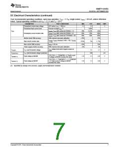
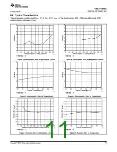
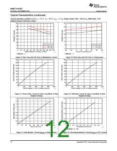
6.6 AC Electrical Characteristics
Over recommended operating conditions, open loop operation, VOUT = 2 VPP single-ended, I(BIAS) = 80 mA unless otherwise
noted. Typical operating condition is at VCC = 2.5 V and TA = 25°C
PARAMETER
TEST CONDITIONS
MIN
TYP
MAX
UNIT
Gbps
dB
TX INPUT SPECIFICATIONS
CDR lock range
CPRI, Ethernet, SONET, Fibre Channel
0.05 GHz < f ≤ 0.1 GHz
0.1 GHz < f ≤ 5.5 GHz
9.80
20
12
8
11.7
SDD11
Differential input return loss
15
15
5.5 GHz < f < 12 GHz
SDD11
SDD11
Differential to common mode conversion
Common mode input return loss
Input AC common mode voltage tolerance
Total Non-DDJ
0.1 GHz < f < 12 GHz
10
3
dB
dB
0.1 GHz < f < 12 GHz
15
mV
Total jitter less ISI
0.45
0.65
UIPP
UIPP
UIPP
mVPP
dB
T(JTX)
S(JTX)
VIN
Total Jitter
Sinusoidal Jitter Tolerance
Differential input voltage swing
EQ high freq boost
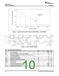
With addition of input jitter, See Figure 1
Maximum setting; 7 GHz
100
6
1000
EQ(boost)
9
TX OUTPUT SPECIFICATIONS
Differential output return loss
Minimum output amplitude
0.01 GHz < f < 12 GHz
12
dB
VO(MIN)
AC Coupled Outputs, 50-Ω single-ended load
0.5
VPP
TX OUTPUT SPECIFICATIONS in SINGLE-ENDED MODE of OPERATION (TXMODE = 1)
VO(MAX)
Maximum output amplitude
Output amplitude stability
High Cross Point Control Range
Low Cross Point Control Range
Cross Point Stability
AC Coupled Outputs, 50-Ω load, single-ended
AC Coupled Outputs, 50-Ω load, single-ended
50-Ω load, single-ended
2
70%
-5
VPP
230
75%
35%
mVPP
50-Ω load, single-ended
40%
5
50-Ω load, single-ended
pp
dB
TXDEADJ[0..3] = 1111, TXPKSEL = 0
TXDEADJ[0..3] = 1111, TXPKSEL = 1
5
6
Output de-emphasis
TX OUTPUT SPECIFICATIONS in DIFFERENTIAL MODE of OPERATION (TXMODE = 0)
VO(MAX)
Maximum output amplitude
Output amplitude stability
High Cross Point Control Range
Low Cross Point Control Range
Cross Point Stability
AC Coupled Outputs, 100-Ω differential load
AC Coupled Outputs, 100-Ω differential load
100-Ω differential load
3.6
65%
–5
VPP
230
75%
35%
mVPP
100-Ω differential load
40%
5
100-Ω differential load
pp
dB
TXDEADJ[0..3] = 1111, TXPKSEL = 0
TXDEADJ[0..3] = 1111, TXPKSEL = 1
5
6
Output de-emphasis
CDR SPECIFICATIONS
BW(TX)
J(PTX)
Jitter Transfer Bandwidth
9.95 Gbps, PRBS31
8
1
MHz
dB
Jitter Peaking
> 120 kHz
JGEN(rms)
JGEN(PP)
Random RMS jitter generation
Total jitter generation
Clock pattern, 50 kHz to 80 MHz
Clock pattern, 50 kHz to 80 MHz, BER = 10-12
6
mUIrms
mUIPP
60
8
Copyright © 2016, Texas Instruments Incorporated

 TI [ TEXAS INSTRUMENTS ]