ONET1131EC
www.ti.com.cn
ZHCSFG0 –SEPTEMBER 2016
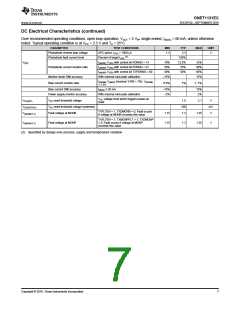
6.7 Timing Requirements
Over recommended operating conditions, typical operating condition is at VCC = 2.5 V and TA = 25°C
MIN
TYP
50
MAX
UNIT
CAPC 0.01 µF, IPD = 500 µA, PD coupling ratio CR = 150,
PDRNG = 01
t(APC)
APC time constant
µs
t(INIT1)
t(INIT2)
t(OFF)
Power-on to initialize
Initialize to transmit
Transmitter disable time
Disable negate time
DIS pulse width
Power-on to registers ready to be loaded
Register load STOP command to part ready to transmit valid data
Rising edge of DIS to I(BIAS) ≤ 0.1 × I(BIAS-NOMINAL)
Falling edge of DIS to I(BIAS) ≥ 0.9 × I(BIAS-NOMINAL)
Time DIS must held high to reset part
0.2
1
2
5
1
ms
ms
µs
1
t(ON)
ms
ns
t(RESET)
t(FAULT)
100
Fault assert time
Time from fault condition to FLT high
50
µs
OUTPUT SPECIFICATIONS in SINGLE-ENDED MODE of OPERATION (TXMODE = 1)
tR(OUTTX)
tF(OUTTX)
Output rise time
Output fall time
20% - 80%, AC Coupled Outputs, 50-Ω load, single-ended
20% - 80%, AC Coupled Outputs, 50-Ω load, single-ended
30
30
42
42
ps
ps
TXEQ_DIS = 1, 11.3 Gbps, PRBS9 pattern, 150-mVpp,
600-mVpp, 1200-mVpp differential input voltage
4
7
12
ISI(TX)
Intersymbol interference
ps
TXEQ_DIS = 0, 11.3 Gbps, PRBS9 pattern, 150-mVpp,
600-mVpp, 1200-mVpp differential input voltage, maximum
equalization with 18-inch transmission line at the input.
Serial data output random
jitter
R(JTX)
0.4
0.75
psRMS
ps
TXPKSEL = 0
TXPKSEL = 1
28
35
Output de-emphasis width
OUTPUT SPECIFICATIONS in DIFFERENTIAL MODE of OPERATION (TXMODE = 0)
tR(OUTTX)
tF(OUTTX)
Output rise time
Output fall time
20%–80%, AC Coupled Outputs, 100-Ω differential load
20%–80%, AC Coupled Outputs, 100-Ω differential load
30
30
42
42
ps
ps
TXEQ_DIS = 1, 11.3 Gbps, PRBS9 pattern, 150-mVpp,
600-mVpp, 1200-mVpp differential input voltage
4
7
10
ISI(TX)
Intersymbol interference
ps
TXEQ_DIS = 0, 11.3 Gbps, PRBS9 pattern, 150-mVpp,
600-mVpp, 1200-mVpp differential input voltage, maximum
equalization with 18-inch transmission line at the input.
Serial data output random
jitter
R(JTX)
0.4
0.75
psRMS
ps
TXPKSEL = 0
TXPKSEL = 1
28
35
Output Peaking Width
CDR SPECIFICATIONS
t(Lock,TX) CDR Acquisition time
LOL assert time
2
ms
500
μs
Copyright © 2016, Texas Instruments Incorporated
9

 TI [ TEXAS INSTRUMENTS ]