ONET1131EC
www.ti.com.cn
ZHCSFG0 –SEPTEMBER 2016
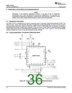
Typical Application, Transmitter Differential Mode (continued)
8.2.1 Design Requirements
Table 26. Design Parameters
PARAMETER
VALUE
Supply voltage
2.5 V
Transmitter input voltage
Transmitter output voltage
100 mVpp to 1000 mVpp differential
1 Vpp to 3.6 Vpp differential
8.2.2 Detailed Design Procedure
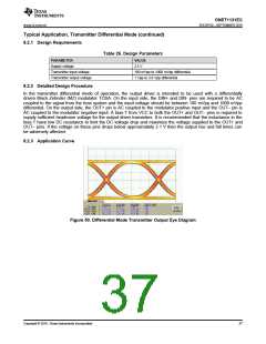
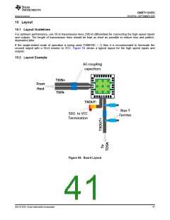
In the transmitter differential mode of operation, the output driver is intended to be used with a differentially
driven Mach Zehnder (MZ) modulator TOSA. On the input side, the DIN+ and DIN- pins are required to be AC
coupled to the signal from the host system and the input voltage should be between 100 mVpp and 1000 mVpp
differential. On the output side, the OUT+ pin is AC coupled to the modulator positive input and the OUT– pin is
AC coupled to the modulator negative input. A bias-T from VCC to both the OUT+ and OUT– pins is required to
supply sufficient headroom voltage for the output driver transistors. It is recommended that the inductance in the
bias-T have low DC resistance to limit the DC voltage drop and maximize the voltage supplied to the OUT+ and
OUT– pins. If the voltage on these pins drops below approximately 2.1 V then the output rise and fall times can
be adversely affected.
8.2.3 Application Curve
Figure 50. Differential Mode Transmitter Output Eye Diagram
Copyright © 2016, Texas Instruments Incorporated
37

 TI [ TEXAS INSTRUMENTS ]