ONET1131EC
ZHCSFG0 –SEPTEMBER 2016
www.ti.com.cn
8.2.4.1 Design Requirements
Table 27. Design Parameters
PARAMETER
VALUE
Supply voltage
2.5 V
Transmitter input voltage
Transmitter output voltage
100 mVpp to 1000 mVpp differential
0.5 Vpp to 2 Vpp single-ended
8.2.4.2 Detailed Design Procedure
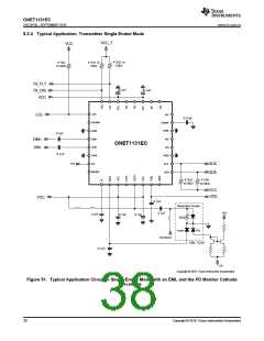
In the transmitter single-ended mode of operation, the output driver is intended to be used with a single-ended
driven Electroabsorptive Modulated Laser (EML) TOSA. On the input side, the DIN+ and DIN– pins are required
to be AC coupled to the signal from the host system and the input voltage should be between 100 mVpp and
1000 mVpp differential. On the output side, it is recommended that the OUT+ pin is AC coupled to the modulator
input and the OUT– pin can be left unterminated or terminated to VCC through a 50-Ω resistor. A bias-T from
VCC to the OUT+ pin is required to supply sufficient headroom voltage for the output driver transistors. It is
recommended that the inductance in the bias-T have low DC resistance to limit the DC voltage drop and
maximize the voltage supplied to the TXOUT+ pin. If the voltage on this pins drops below approximately 2.1V
then the output rise and fall times can be adversely affected.
8.2.4.3 Application Curves
Figure 53. Single-Ended Mode Transmitter Output Eye Diagram
9 Power Supply Recommendations
The ONET1131EC is designed to operate from an input supply voltage range between 2.37 V and 2.63 V. To
reduce digital coupling into the analog circuitry, there are separate supplies for the transmitter, and digital
circuitry. VCC is used to supply power to the transmitter, and VDD is used to supply power to the digital block.
Power supply decoupling capacitors should be placed as close as possible to the respective power supply pins.
40
Copyright © 2016, Texas Instruments Incorporated

 TI [ TEXAS INSTRUMENTS ]