OMAP-L137 Low-Power Applications Processor
SPRS563A–SEPTEMBER 2008–REVISED OCTOBER 2008
www.ti.com
6 Peripheral Information and Electrical Specifications
6.1 Parameter Information
6.1.1 Parameter Information Device-Specific Information
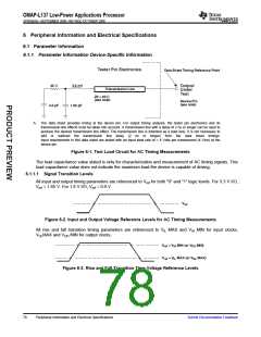
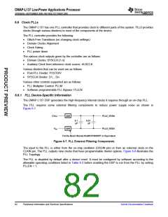
Tester Pin Electronics
Data Sheet Timing Reference Point
42 Ω
3.5 nH
Output
Under
Test
Transmission Line
Z0 = 50 Ω
(see note)
Device Pin
(see note)
4.0 pF
1.85 pF
A. The data sheet provides timing at the device pin. For output timing analysis, the tester pin electronics and its
transmission line effects must be taken into account. A transmission line with a delay of 2 ns or longer can be used to
produce the desired transmission line effect. The transmission line is intended as a load only. It is not necessary to
add or subtract the transmission line delay (2 ns or longer) from the data sheet timings.
Input requirements in this data sheet are tested with an input slew rate of < 4 Volts per nanosecond (4 V/ns) at the
device pin.
Figure 6-1. Test Load Circuit for AC Timing Measurements
The load capacitance value stated is only for characterization and measurement of AC timing signals. This
load capacitance value does not indicate the maximum load the device is capable of driving.
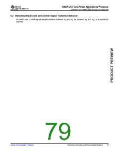
6.1.1.1 Signal Transition Levels
All input and output timing parameters are referenced to Vref for both "0" and "1" logic levels. For 3.3 V I/O,
Vref = 1.65 V. For 1.8 V I/O, Vref = 0.9 V.
V
ref
Figure 6-2. Input and Output Voltage Reference Levels for AC Timing Measurements
All rise and fall transition timing parameters are referenced to VIL MAX and VIH MIN for input clocks,
VOLMAX and VOH MIN for output clocks.
V
ref
= V MIN (or V MIN)
IH OH
V
ref
= V MAX (or V MAX)
IL OL
Figure 6-3. Rise and Fall Transition Time Voltage Reference Levels
78
Peripheral Information and Electrical Specifications
Submit Documentation Feedback

 TI [ TEXAS INSTRUMENTS ]