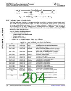
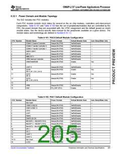
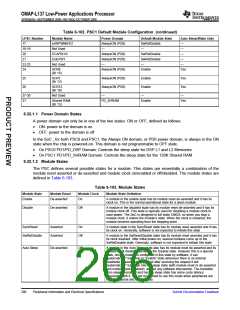
OMAP-L137 Low-Power Applications Processor
www.ti.com
SPRS563A–SEPTEMBER 2008–REVISED OCTOBER 2008
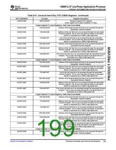
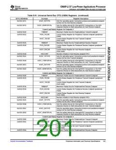
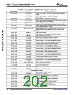
Table 6-91. Universal Serial Bus OTG (USB0) Registers (continued)
BYTE ADDRESS
Acronym
PEND1
Register Description
Queue Pending Register 1
0x01E0 4094
0x01E0 5000
0x01E0 5004
0x01E0 5010
0x01E0 5014
. . .
QMEMRBASE[0]
QMEMRCTRL[0]
QMEMRBASE[1]
QMEMRCTRL[1]
. . .
Memory Region 0 Base Address Register
Memory Region 0 Control Register
Memory Region 1 Base Address Register
Memory Region 1 Control Register
. . .
0x01E0 5070
0x01E0 5074
0x01E0 600C
0x01E0 601C
. . .
QMEMRBASE[7]
QMEMRCTRL[7]
CTRLD[0]
Memory Region 7 Base Address Register
Memory Region 7 Control Register
Queue Manager Queue 0 Control Register D
Queue Manager Queue 1 Control Register D
. . .
CTRLD[1]
. . .
0x01E0 63FC
0x01E0 6800
0x01E0 6804
0x01E0 6808
0x01E0 6810
0x01E0 6814
0x01E0 6818
. . .
CTRLD[63]
QSTATA[0]
QSTATB[0]
QSTATC[0]
QSTATA[1]
QSTATB[1]
QSTATC[1]
. . .
Queue Manager Queue 63 Status Register D
Queue Manager Queue 0 Status Register A
Queue Manager Queue 0 Status Register B
Queue Manager Queue 0 Status Register C
Queue Manager Queue 1 Status Register A
Queue Manager Queue 1 Status Register B
Queue Manager Queue 1 Status Register C
. . .
0x01E0 6BF0
0x01E0 6BF4
0x01E0 6BF8
QSTATA[63]
QSTATB[63]
QSTATC[63]
Queue Manager Queue 63 Status Register A
Queue Manager Queue 63 Status Register B
Queue Manager Queue 63 Status Register C
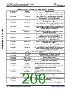
6.27.1 USB2.0 Electrical Data/Timing
Table 6-92. Switching Characteristics Over Recommended Operating Conditions for USB2.0 (see
Figure 6-65)
LOW SPEED
1.5 Mbps
FULL SPEED
12 Mbps
HIGH SPEED
480 Mbps
NO.
PARAMETER
UNIT
MIN
75
MAX
MIN
4
MAX
MIN
0.5
0.5
–
MAX
1
2
3
4
5
tr(D)
Rise time, USB_DP and USB_DM signals(1)
Fall time, USB_DP and USB_DM signals(1)
Rise/Fall time, matching(2)
Output signal cross-over voltage(1)
Source (Host) Driver jitter, next transition
Function Driver jitter, next transition
Source (Host) Driver jitter, paired transition(4)
Function Driver jitter, paired transition
Pulse duration, EOP transmitter
Pulse duration, EOP receiver
300
300
120
2
20
20
111
2
ns
ns
%
tf(D)
75
4
trfM
80
90
1.3
–
–
VCRS
1.3
–
V
tjr(source)NT
tjr(FUNC)NT
tjr(source)PT
tjr(FUNC)PT
tw(EOPT)
tw(EOPR)
t(DRATE)
2
2
(3)ns
ns
ns
ns
ns
ns
(3)
(3)
(3)
25
2
6
1
1
10
1
7
8
9
1250
670
1500
160
82
175
–
–
–
Data Rate
1.5
–
12
480 Mb/s
10 ZDRV
11 ZINP
Driver Output Resistance
–
40.5
49.5
40.5
-
49.5
-
Ω
Ω
Receiver Input Impedance
100k
100k
(1) Low Speed: CL = 200 pF, Full Speed: CL = 50 pF, High Speed: CL = 50 pF
(2) tRFM = (tr/tf) x 100. [Excluding the first transaction from the Idle state.]
(3) For more detailed information, see the Universal Serial Bus Specification Revision 2.0, Chapter 7. Electrical.
(4) tjr = tpx(1) - tpx(0)
Submit Documentation Feedback
Peripheral Information and Electrical Specifications
203

 TI [ TEXAS INSTRUMENTS ]