OMAP-L137 Low-Power Applications Processor
SPRS563A–SEPTEMBER 2008–REVISED OCTOBER 2008
www.ti.com
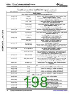
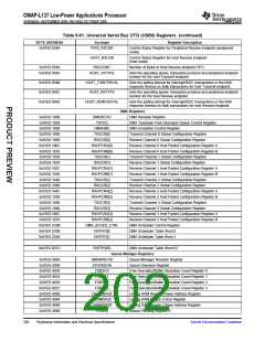
Table 6-91. Universal Serial Bus OTG (USB0) Registers (continued)
BYTE ADDRESS
Acronym
Register Description
0x01E0 0546
PERI_RXCSR
Control Status Register for Peripheral Receive Endpoint (peripheral
mode)
HOST_RXCSR
Control Status Register for Host Receive Endpoint
(host mode)
0x01E0 0548
0x01E0 054A
RXCOUNT
Number of Bytes in Host Receive endpoint FIFO
HOST_TXTYPE
Sets the operating speed, transaction protocol and peripheral endpoint
number for the host Transmit endpoint.
0x01E0 054B
0x01E0 054C
0x01E0 054D
HOST_TXINTERVAL
HOST_RXTYPE
Sets the polling interval for Interrupt/ISOC transactions or the NAK
response timeout on Bulk transactions for host Transmit endpoint.
Sets the operating speed, transaction protocol and peripheral endpoint
number for the host Receive endpoint.
HOST_RXINTERVAL
Sets the polling interval for Interrupt/ISOC transactions or the NAK
response timeout on Bulk transactions for host Receive endpoint.
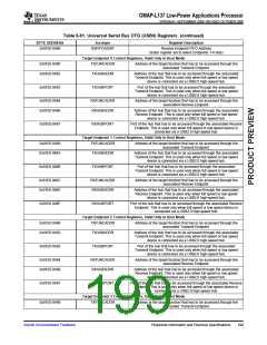
DMA Registers
0x01E0 1000
0x01E0 1004
0x01E0 1008
0x01E0 1800
0x01E0 1808
0x01E0 180C
0x01E0 1810
0x01E0 1820
0x01E0 1828
0x01E0 182C
0x01E0 1830
0x01E0 1840
0x01E0 1848
0x01E0 184C
0x01E0 1850
0x01E0 1860
0x01E0 1868
0x01E0 186C
0x01E0 1870
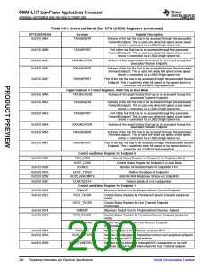
0x01E0 2C00
0x01E0 2D00
0x01E0 2D04
. . .
DMAREVID
TDFDQ
DMA Revision Register
DMA Teardown Free Descriptor Queue Control Register
DMA Emulation Control Register
DMAEMU
TXGCR[0]
Transmit Channel 0 Global Configuration Register
Receive Channel 0 Global Configuration Register
Receive Channel 0 Host Packet Configuration Register A
Receive Channel 0 Host Packet Configuration Register B
Transmit Channel 1 Global Configuration Register
Receive Channel 1 Global Configuration Register
Receive Channel 1 Host Packet Configuration Register A
Receive Channel 1 Host Packet Configuration Register B
Transmit Channel 2 Global Configuration Register
Receive Channel 2 Global Configuration Register
Receive Channel 2 Host Packet Configuration Register A
Receive Channel 2 Host Packet Configuration Register B
Transmit Channel 3 Global Configuration Register
Receive Channel 3 Global Configuration Register
Receive Channel 3 Host Packet Configuration Register A
Receive Channel 3 Host Packet Configuration Register B
DMA Scheduler Control Register
RXGCR[0]
RXHPCRA[0]
RXHPCRB[0]
TXGCR[1]
RXGCR[1]
RXHPCRA[1]
RXHPCRB[1]
TXGCR[2]
RXGCR[2]
RXHPCRA[2]
RXHPCRB[2]
TXGCR[3]
RXGCR[3]
RXHPCRA[3]
RXHPCRB[3]
DMA_SCHED_CTRL
ENTRY[0]
DMA Scheduler Table Word 0
ENTRY[1]
DMA Scheduler Table Word 1
. . .
. . .
0x01E0 2DFC
ENTRY[63]
DMA Scheduler Table Word 63
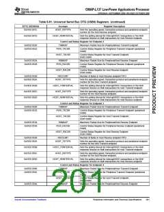
Queue Manager Registers
0x01E0 4000
0x01E0 4008
0x01E0 4020
0x01E0 4024
0x01E0 4028
0x01E0 402C
0x01E0 4080
0x01E0 4084
0x01E0 4088
0x01E0 4090
QMGRREVID
DIVERSION
FDBSC0
Queue Manager Revision Register
Queue Diversion Register
Free Descriptor/Buffer Starvation Count Register 0
Free Descriptor/Buffer Starvation Count Register 1
Free Descriptor/Buffer Starvation Count Register 2
Free Descriptor/Buffer Starvation Count Register 3
Linking RAM Region 0 Base Address Register
Linking RAM Region 0 Size Register
FDBSC1
FDBSC2
FDBSC3
LRAM0BASE
LRAM0SIZE
LRAM1BASE
PEND0
Linking RAM Region 1 Base Address Register
Queue Pending Register 0
202
Peripheral Information and Electrical Specifications
Submit Documentation Feedback

 TI [ TEXAS INSTRUMENTS ]