MSP430F530x, MSP430F5310
SLAS677B –SEPTEMBER 2010–REVISED MARCH 2011
www.ti.com
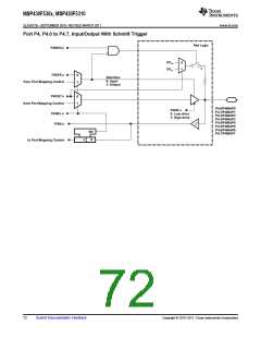
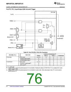
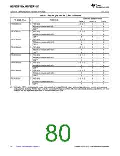
Port P5, P5.3, Input/Output With Schmitt Trigger
Pad Logic
To XT2
P5REN.3
DVSS
DVCC
0
1
1
P5DIR.3
0
1
P5OUT.3
0
1
Module X OUT
P5.3/XT2OUT
P5DS.3
0: Low drive
1: High drive
P5SEL.3
P5IN.3
Bus
Keeper
EN
D
Module X IN
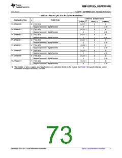
Table 51. Port P5 (P5.2, P5.3) Pin Functions
CONTROL BITS/SIGNALS(1)
PIN NAME (P5.x)
x
FUNCTION
P5DIR.x
P5SEL.2
P5SEL.3
XT2BYPASS
P5.2/XT2IN
2
P5.2 (I/O)
I: 0; O: 1
0
1
1
0
1
1
X
X
X
X
X
X
X
0
1
X
0
1
XT2IN crystal mode(2)
XT2IN bypass mode(2)
P5.3 (I/O)
XT2OUT crystal mode(3)
P5.3 (I/O)(3)
X
X
P5.3/XT2OUT
3
I: 0; O: 1
X
X
(1) X = Don't care
(2) Setting P5SEL.2 causes the general-purpose I/O to be disabled. Pending the setting of XT2BYPASS, P5.2 is configured for crystal
mode or bypass mode.
(3) Setting P5SEL.2 causes the general-purpose I/O to be disabled in crystal mode. When using bypass mode, P5.3 can be used as
general-purpose I/O.
76
Submit Documentation Feedback
Copyright © 2010–2011, Texas Instruments Incorporated

 TI [ TEXAS INSTRUMENTS ]