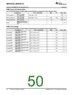
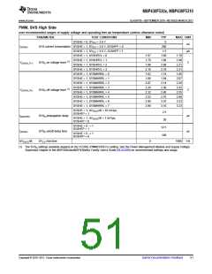
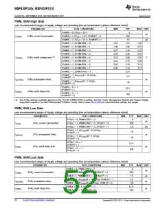
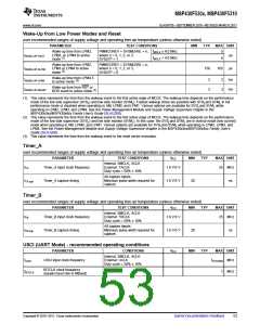
MSP430F530x, MSP430F5310
SLAS677B –SEPTEMBER 2010–REVISED MARCH 2011
www.ti.com
MAX UNIT
USCI (UART Mode)
over recommended ranges of supply voltage and operating free-air temperature (unless otherwise noted)
PARAMETER
TEST CONDITIONS
VCC
2.2 V
3 V
MIN
50
TYP
600
ns
(1)
tτ
UART receive deglitch time
50
600
(1) Pulses on the UART receive input (UCxRX) shorter than the UART receive deglitch time are suppressed. To ensure that pulses are
correctly recognized their width should exceed the maximum specification of the deglitch time.
USCI (SPI Master Mode) - recommended operating conditions
PARAMETER
CONDITIONS
VCC
MIN
TYP
MAX UNIT
Internal: SMCLK, ACLK
Duty cycle = 50% ± 10%
fUSCI
USCI input clock frequency
fSYSTEM MHz
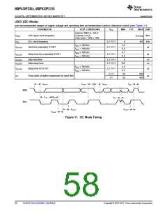
USCI (SPI Master Mode)
over recommended ranges of supply voltage and operating free-air temperature (unless otherwise noted)
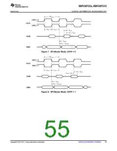
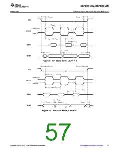
(see Note (1), Figure 7 and Figure 8)
PARAMETER
TEST CONDITIONS
VCC
MIN
TYP
MAX UNIT
SMCLK, ACLK
Duty cycle = 50% ± 10%
fUSCI
USCI input clock frequency
fSYSTEM MHz
1.8 V
3 V
55
38
30
25
0
PMMCOREV = 0
ns
ns
ns
ns
tSU,MI
SOMI input data setup time
SOMI input data hold time
SIMO output data valid time
SIMO output data hold time
2.4 V
3 V
PMMCOREV = 3
PMMCOREV = 0
PMMCOREV = 3
1.8 V
3 V
0
tHD,MI
2.4 V
3 V
0
0
1.8 V
3 V
20
ns
18
UCLK edge to SIMO valid,
CL = 20 pF, PMMCOREV = 0
(2)
tVALID,MO
2.4 V
3 V
16
ns
15
UCLK edge to SIMO valid,
CL = 20 pF, PMMCOREV = 3
1.8 V
3 V
-10
-8
CL = 20 pF, PMMCOREV = 0
CL = 20 pF, PMMCOREV = 3
ns
ns
(3)
tHD,MO
2.4 V
3 V
-10
-8
(1) fUCxCLK = 1/2tLO/HI with tLO/HI ≥ max(tVALID,MO(USCI) + tSU,SI(Slave), tSU,MI(USCI) + tVALID,SO(Slave)).
For the slave's parameters tSU,SI(Slave) and tVALID,SO(Slave) see the SPI parameters of the attached slave.
(2) Specifies the time to drive the next valid data to the SIMO output after the output changing UCLK clock edge. Refer to the timing
diagrams in Figure 7 and Figure 8.
(3) Specifies how long data on the SIMO output is valid after the output changing UCLK clock edge. Negative values indicate that the data
on the SIMO output can become invalid before the output changing clock edge observed on UCLK. Refer to the timing diagrams in
Figure 7 and Figure 8.
54
Submit Documentation Feedback
Copyright © 2010–2011, Texas Instruments Incorporated

 TI [ TEXAS INSTRUMENTS ]