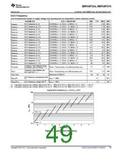
MSP430F530x, MSP430F5310
www.ti.com
SLAS677B –SEPTEMBER 2010–REVISED MARCH 2011
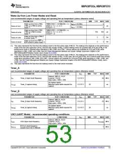
Wake-Up from Low Power Modes and Reset
over recommended ranges of supply voltage and operating free-air temperature (unless otherwise noted)
PARAMETER
TEST CONDITIONS
MIN
TYP
MAX UNIT
Wake-up time from LPM2,
LPM3, or LPM4 to active
mode
PMMCOREV = SVSMLRRL = n,
where n = 0, 1, 2, or 3,
SVSLFP = 1
f
MCLK ≥ 4.0 MHz
MCLK < 4.0 MHz
5
tWAKE-UP-FAST
µs
(1)
f
6
Wake-up time from LPM2,
LPM3 or LPM4 to active
mode
PMMCOREV = SVSMLRRL = n,
where n = 0, 1, 2, or 3,
SVSLFP = 0
tWAKE-UP-SLOW
150
165
µs
(2)
Wake-up time from LPM4.5
to active mode
tWAKE-UP-LPM5
tWAKE-UP-RESET
2
2
3
3
ms
ms
(3)
Wake-up time from RST or
BOR event to active mode
(3)
(1) This value represents the time from the wakeup event to the first active edge of MCLK. The wakeup time depends on the performance
mode of the low side supervisor (SVSL) and low side monitor (SVML). Fastest wakeup times are possible with SVSLand SVML in full
performance mode or disabled when operating in AM, LPM0, and LPM1. Various options are available for SVSLand SVML while
operating in LPM2, LPM3, and LPM4. See the Power Management Module and Supply Voltage Supervisor chapter in the
MSP430x5xx/MSP430x6xx Family User's Guide (SLAU208).
(2) This value represents the time from the wakeup event to the first active edge of MCLK. The wakeup time depends on the performance
mode of the low side supervisor (SVSL) and low side monitor (SVML). In this case, the SVSLand SVML are in normal mode (low current)
mode when operating in AM, LPM0, and LPM1. Various options are available for SVSLand SVML while operating in LPM2, LPM3, and
LPM4. See the Power Management Module and Supply Voltage Supervisor chapter in the MSP430x5xx/MSP430x6xx Family User's
Guide (SLAU208).
(3) This value represents the time from the wakeup event to the reset vector execution.
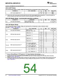
Timer_A
over recommended ranges of supply voltage and operating free-air temperature (unless otherwise noted)
PARAMETER
TEST CONDITIONS
VCC
MIN
TYP
MAX UNIT
Internal: SMCLK, ACLK
fTA
Timer_A input clock frequency
External: TACLK
1.8 V/3 V
25 MHz
Duty cycle = 50% ± 10%
All capture inputs.
tTA,cap
Timer_A capture timing
Minimum pulse width required for
capture.
1.8 V/3 V
20
ns
Timer_B
over recommended ranges of supply voltage and operating free-air temperature (unless otherwise noted)
PARAMETER
TEST CONDITIONS
VCC
MIN
TYP
MAX UNIT
Internal: SMCLK, ACLK
fTB
Timer_B input clock frequency
External: TBCLK
1.8 V/3 V
25 MHz
Duty cycle = 50% ± 10%
All capture inputs.
tTB,cap
Timer_B capture timing
Minimum pulse width required for
capture.
1.8 V/3 V
20
ns
USCI (UART Mode) - recommended operating conditions
PARAMETER
CONDITIONS
VCC
MIN
TYP
MAX UNIT
Internal: SMCLK, ACLK
External: UCLK
fUSCI
USCI input clock frequency
fSYSTEM MHz
Duty cycle = 50% ± 10%
BITCLK clock frequency
(equals baud rate in MBaud)
fBITCLK
1
MHz
Copyright © 2010–2011, Texas Instruments Incorporated
Submit Documentation Feedback
53

 TI [ TEXAS INSTRUMENTS ]