MSP430G2x53
MSP430G2x13
SLAS735A –APRIL 2011–REVISED MAY 2011
www.ti.com
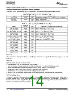
Calibration Data Stored in Information Memory Segment A
Calibration data is stored for both the DCO and for ADC10 organized in a tag-length-value structure.
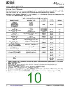
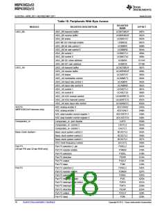
Table 10. Tags Used by the ADC Calibration Tags
NAME
ADDRESS
0x10F6
0x10DA
-
VALUE
0x01
DESCRIPTION
TAG_DCO_30
TAG_ADC10_1
TAG_EMPTY
DCO frequency calibration at VCC = 3 V and TA = 30°C at calibration
ADC10_1 calibration tag
0x08
0xFE
Identifier for empty memory areas
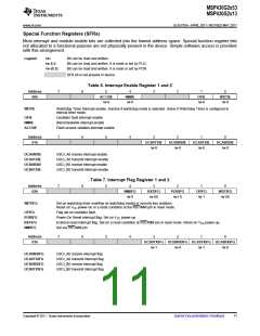
Table 11. Labels Used by the ADC Calibration Tags
ADDRESS
LABEL
SIZE
CONDITION AT CALIBRATION / DESCRIPTION
OFFSET
0x0010
0x000E
0x000C
0x000A
0x0008
0x0006
0x0004
0x0002
0x0009
0x0008
0x0007
0x0006
0x0005
0x0004
0x0003
0x0002
CAL_ADC_25T85
CAL_ADC_25T30
word
word
word
word
word
word
word
word
byte
byte
byte
byte
byte
byte
byte
byte
INCHx = 0x1010, REF2_5 = 1, TA = 85°C
INCHx = 0x1010, REF2_5 = 1, TA = 30°C
CAL_ADC_25VREF_FACTOR
CAL_ADC_15T85
REF2_5 = 1, TA = 30°C, IVREF+ = 1 mA
INCHx = 0x1010, REF2_5 = 0, TA = 85°C
CAL_ADC_15T30
INCHx = 0x1010, REF2_5 = 0, TA = 30°C
CAL_ADC_15VREF_FACTOR
CAL_ADC_OFFSET
CAL_ADC_GAIN_FACTOR
CAL_BC1_1MHZ
REF2_5 = 0, TA = 30°C, IVREF+ = 0.5 mA
External VREF = 1.5 V, fADC10CLK = 5 MHz
External VREF = 1.5 V, fADC10CLK = 5 MHz
-
-
-
-
-
-
-
-
CAL_DCO_1MHZ
CAL_BC1_8MHZ
CAL_DCO_8MHZ
CAL_BC1_12MHZ
CAL_DCO_12MHZ
CAL_BC1_16MHZ
CAL_DCO_16MHZ
Brownout
The brownout circuit is implemented to provide the proper internal reset signal to the device during power on and
power off.
Digital I/O
Up to three 8-bit I/O ports are implemented:
•
•
•
•
•
•
All individual I/O bits are independently programmable.
Any combination of input, output, and interrupt condition (port P1 and port P2 only) is possible.
Edge-selectable interrupt input capability for all bits of port P1 and port P2 (if available).
Read/write access to port-control registers is supported by all instructions.
Each I/O has an individually programmable pullup/pulldown resistor.
Each I/O has an individually programmable pin oscillator enable bit to enable low-cost touch sensing.
WDT+ Watchdog Timer
The primary function of the watchdog timer (WDT+) module is to perform a controlled system restart after a
software problem occurs. If the selected time interval expires, a system reset is generated. If the watchdog
function is not needed in an application, the module can be disabled or configured as an interval timer and can
generate interrupts at selected time intervals.
14
Submit Documentation Feedback
Copyright © 2011, Texas Instruments Incorporated

 TI [ TEXAS INSTRUMENTS ]