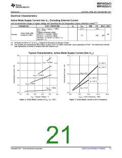
MSP430G2x53
MSP430G2x13
www.ti.com
SLAS735A –APRIL 2011–REVISED MAY 2011
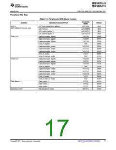
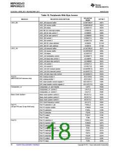
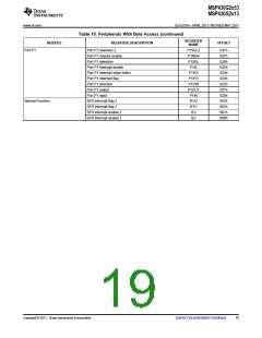
Peripheral File Map
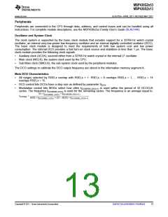
Table 14. Peripherals With Word Access
REGISTER
OFFSET
NAME
MODULE
REGISTER DESCRIPTION
ADC10
ADC data transfer start address
ADC memory
ADC10SA
ADC10MEM
ADC10CTL1
ADC10CTL0
TACCR2
TACCR1
TACCR0
TAR
1BCh
1B4h
(MSP430G2x53 devices only)
ADC control register 1
ADC control register 0
Capture/compare register
Capture/compare register
Capture/compare register
Timer_A register
1B2h
1B0h
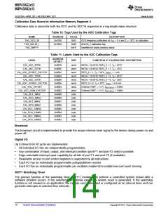
Timer1_A3
0196h
0194h
0192h
0190h
0186h
0184h
0182h
0180h
011Eh
0176h
0174h
0172h
0170h
0166h
0164h
0162h
0160h
012Eh
012Ch
012Ah
0128h
0120h
Capture/compare control
Capture/compare control
Capture/compare control
Timer_A control
TACCTL2
TACCTL1
TACCTL0
TACTL
Timer_A interrupt vector
Capture/compare register
Capture/compare register
Capture/compare register
Timer_A register
TAIV
Timer0_A3
TACCR2
TACCR1
TACCR0
TAR
Capture/compare control
Capture/compare control
Capture/compare control
Timer_A control
TACCTL2
TACCTL1
TACCTL0
TACTL
Timer_A interrupt vector
Flash control 3
TAIV
Flash Memory
FCTL3
Flash control 2
FCTL2
Flash control 1
FCTL1
Watchdog Timer+
Watchdog/timer control
WDTCTL
Copyright © 2011, Texas Instruments Incorporated
Submit Documentation Feedback
17

 TI [ TEXAS INSTRUMENTS ]