MSP430G2x53
MSP430G2x13
SLAS735A –APRIL 2011–REVISED MAY 2011
www.ti.com
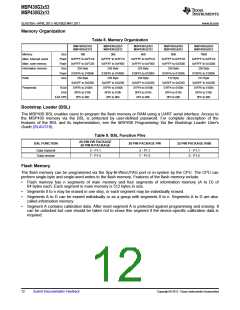
Memory Organization
Table 8. Memory Organization
MSP430G2153
MSP430G2113
MSP430G2253
MSP430G2213
MSP430G2353
MSP430G2313
MSP430G2453
MSP430G2413
MSP430G2553
MSP430G2513
Memory
Size
Flash
Flash
Size
1kB
2kB
4kB
8kB
16kB
Main: interrupt vector
Main: code memory
Information memory
0xFFFF to 0xFFC0
0xFFFF to 0xFC00
256 Byte
0xFFFF to 0xFFC0
0xFFFF to 0xF800
256 Byte
0xFFFF to 0xFFC0
0xFFFF to 0xF000
256 Byte
0xFFFF to 0xFFC0
0xFFFF to 0xE000
256 Byte
0xFFFF to 0xFFC0
0xFFFF to 0xC000
256 Byte
Flash
Size
010FFh to 01000h
256 Byte
010FFh to 01000h
256 Byte
010FFh to 01000h
256 Byte
010FFh to 01000h
512 Byte
010FFh to 01000h
512 Byte
RAM
0x02FF to 0x0200
01FFh to 0100h
0FFh to 010h
0Fh to 00h
0x02FF to 0x0200
01FFh to 0100h
0FFh to 010h
0Fh to 00h
0x02FF to 0x0200
01FFh to 0100h
0FFh to 010h
0Fh to 00h
0x03FF to 0x0200
01FFh to 0100h
0FFh to 010h
0Fh to 00h
0x03FF to 0x0200
01FFh to 0100h
0FFh to 010h
0Fh to 00h
Peripherals
16-bit
8-bit
8-bit SFR
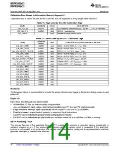
Bootstrap Loader (BSL)
The MSP430 BSL enables users to program the flash memory or RAM using a UART serial interface. Access to
the MSP430 memory via the BSL is protected by user-defined password. For complete description of the
features of the BSL and its implementation, see the MSP430 Programming Via the Bootstrap Loader User's
Guide (SLAU319).
Table 9. BSL Function Pins
20-PIN PW PACKAGE
20-PIN N PACKAGE
BSL FUNCTION
28-PIN PACKAGE PW
32-PIN PACKAGE RHB
Data transmit
Data receive
3 - P1.1
3 - P1.1
7 - P1.5
1 - P1.1
5 - P1.5
7 - P1.5
Flash Memory
The flash memory can be programmed via the Spy-Bi-Wire/JTAG port or in-system by the CPU. The CPU can
perform single-byte and single-word writes to the flash memory. Features of the flash memory include:
•
Flash memory has n segments of main memory and four segments of information memory (A to D) of
64 bytes each. Each segment in main memory is 512 bytes in size.
•
•
Segments 0 to n may be erased in one step, or each segment may be individually erased.
Segments A to D can be erased individually or as a group with segments 0 to n. Segments A to D are also
called information memory.
•
Segment A contains calibration data. After reset segment A is protected against programming and erasing. It
can be unlocked but care should be taken not to erase this segment if the device-specific calibration data is
required.
12
Submit Documentation Feedback
Copyright © 2011, Texas Instruments Incorporated

 TI [ TEXAS INSTRUMENTS ]