MSP430G2x53
MSP430G2x13
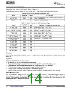
SLAS735A –APRIL 2011–REVISED MAY 2011
www.ti.com
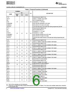
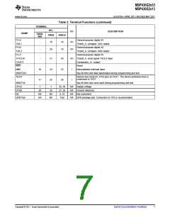
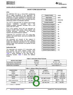
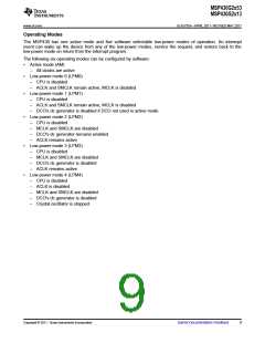
Interrupt Vector Addresses
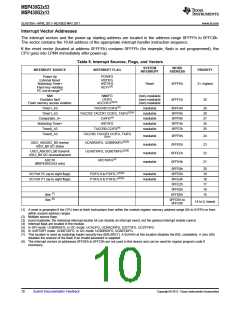
The interrupt vectors and the power-up starting address are located in the address range 0FFFFh to 0FFC0h.
The vector contains the 16-bit address of the appropriate interrupt handler instruction sequence.
If the reset vector (located at address 0FFFEh) contains 0FFFFh (for example, flash is not programmed), the
CPU goes into LPM4 immediately after power-up.
Table 5. Interrupt Sources, Flags, and Vectors
SYSTEM
INTERRUPT
WORD
ADDRESS
INTERRUPT SOURCE
INTERRUPT FLAG
PRIORITY
Power-Up
External Reset
Watchdog Timer+
Flash key violation
PC out-of-range(1)
PORIFG
RSTIFG
WDTIFG
KEYV(2)
Reset
0FFFEh
31, highest
NMI
Oscillator fault
Flash memory access violation
NMIIFG
OFIFG
(non)-maskable
(non)-maskable
(non)-maskable
0FFFCh
30
ACCVIFG(2)(3)
Timer1_A3
Timer1_A3
TACCR0 CCIFG(4)
TACCR2 TACCR1 CCIFG, TAIFG(2)(4)
CAIFG(4)
maskable
maskable
maskable
maskable
maskable
0FFFAh
0FFF8h
0FFF6h
0FFF4h
0FFF2h
29
28
27
26
25
Comparator_A+
Watchdog Timer+
Timer0_A3
WDTIFG
TACCR0 CCIFG(4)
Timer0_A3
TACCR2 TACCR1 CCIFG, TAIFG
maskable
maskable
maskable
maskable
0FFF0h
0FFEEh
0FFECh
0FFEAh
24
23
22
21
(5)(4)
USCI_A0/USCI_B0 receive
USCI_B0 I2C status
UCA0RXIFG, UCB0RXIFG(2)(5)
UCA0TXIFG, UCB0TXIFG(2)(6)
ADC10IFG(4)
USCI_A0/USCI_B0 transmit
USCI_B0 I2C receive/transmit
ADC10
(MSP430G2x53 only)
0FFE8h
0FFE6h
0FFE4h
0FFE2h
0FFE0h
0FFDEh
20
19
18
17
16
15
I/O Port P2 (up to eight flags)
I/O Port P1 (up to eight flags)
P2IFG.0 to P2IFG.7(2)(4)
P1IFG.0 to P1IFG.7(2)(4)
maskable
maskable
(7)
See
(8)
See
0FFDEh to
0FFC0h
14 to 0, lowest
(1) A reset is generated if the CPU tries to fetch instructions from within the module register memory address range (0h to 01FFh) or from
within unused address ranges.
(2) Multiple source flags
(3) (non)-maskable: the individual interrupt-enable bit can disable an interrupt event, but the general interrupt enable cannot.
(4) Interrupt flags are located in the module.
(5) In SPI mode: UCB0RXIFG. In I2C mode: UCALIFG, UCNACKIFG, ICSTTIFG, UCSTPIFG.
(6) In UART/SPI mode: UCB0TXIFG. In I2C mode: UCB0RXIFG, UCB0TXIFG.
(7) This location is used as bootstrap loader security key (BSLSKEY). A 0xAA55 at this location disables the BSL completely. A zero (0h)
disables the erasure of the flash if an invalid password is supplied.
(8) The interrupt vectors at addresses 0FFDEh to 0FFC0h are not used in this device and can be used for regular program code if
necessary.
10
Submit Documentation Feedback
Copyright © 2011, Texas Instruments Incorporated

 TI [ TEXAS INSTRUMENTS ]