MSP430FR573x
MSP430FR572x
SLAS639D –JULY 2011–REVISED AUGUST 2012
www.ti.com
CAUTION
CAUTION
These products use FRAM nonvolatile memory technology. FRAM retention is sensitive to extreme temperatures, such
as those experienced during reflow or hand soldering. See Absolute Maximum Ratings for more information.
System-level ESD protection must be applied in compliance with the device-level ESD specification to prevent electrical
overstress or disturb of data or code memory. See the application report MSP430™ System-Level ESD Considerations
(SLAA530) for more information.
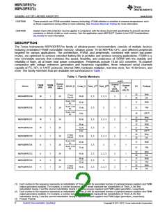
DESCRIPTION
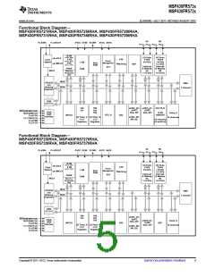
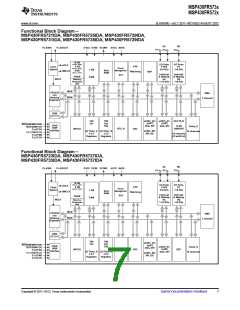
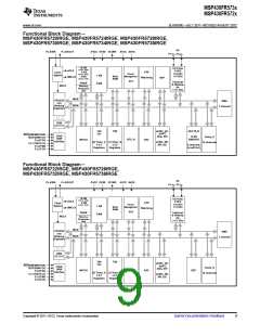
The Texas Instruments MSP430FR57xx family of ultralow-power microcontrollers consists of multiple devices
featuring embedded FRAM nonvolatile memory, ultralow power 16-bit MSP430 CPU, and different peripherals
targeted for various applications. The architecture, FRAM, and peripherals, combined with seven low-power
modes, are optimized to achieve extended battery life in portable and wireless sensing applications. FRAM is a
new nonvolatile memory that combines the speed, flexibility, and endurance of SRAM with the stability and
reliability of flash, all at lower total power consumption. Peripherals include 10-bit A/D converter, 16-channel
comparator with voltage reference generation and hysteresis capabilities, three enhanced serial channels
capable of I2C, SPI, or UART protocols, internal DMA, hardware multiplier, real-time clock, five 16-bit timers, and
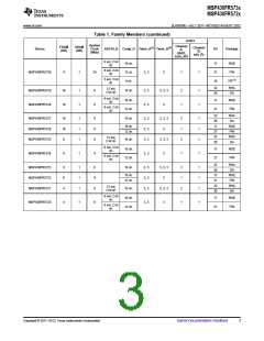
more. The family members that are available are summarized in Table 1.
Table 1. Family Members
eUSCI
System
Clock
(MHz)
Channel
A:
UART,
IrDA, SPI
FRAM
(KB)
SRAM
(KB)
Device
ADC10_B Comp_D Timer_A(1) Timer_B(2)
I/O
Package
Channel
B:
SPI, I2C
32
30
RHA
DA
12 ext,
2 int ch.
MSP430FR5739
16
16
1
1
24
24
16 ch.
3, 3
3, 3
3, 3, 3
2
1
1
1
6 ext, 2 int
ch.
10 ch.
12 ch.
9 ch.
17
21
16
RGE
PW
8 ext, 2 int
ch.
MSP430FR5738
3
5 ext, 2 int
ch.
YFF(3)
32
30
17
21
16
32
30
RHA
DA
MSP430FR5737
MSP430FR5736
MSP430FR5735
16
16
8
1
1
1
24
24
24
16 ch.
3, 3
3, 3
3, 3
3, 3, 3
3
2
1
2
1
1
1
10 ch.
12 ch.
9 ch.
RGE
PW
YFF(3)
RHA
DA
12 ext,
2 int ch.
16 ch.
3, 3, 3
6 ext, 2 int
ch.
10 ch.
12 ch.
17
21
RGE
PW
MSP430FR5734
8
1
24
3, 3
3
1
1
8 ext, 2 int
ch.
32
30
17
21
32
30
RHA
DA
MSP430FR5733
MSP430FR5732
MSP430FR5731
8
8
4
1
1
1
24
24
24
16 ch.
3, 3
3, 3
3, 3
3, 3, 3
3
2
1
2
1
1
1
10 ch.
12 ch.
RGE
PW
RHA
DA
12 ext,
2 int ch.
16 ch.
3, 3, 3
(1) Each number in the sequence represents an instantiation of Timer_A with its associated number of capture/compare registers and PWM
output generators available. For example, a number sequence of 3, 5 would represent two instantiations of Timer_A, the first
instantiation having 3 and the second instantiation having 5 capture/compare registers and PWM output generators, respectively.
(2) Each number in the sequence represents an instantiation of Timer_B with its associated number of capture/compare registers and PWM
output generators available. For example, a number sequence of 3, 5 would represent two instantiations of Timer_B, the first
instantiation having 3 and the second instantiation having 5 capture/compare registers and PWM output generators, respectively.
(3) Product Preview
2
Submit Documentation Feedback
Copyright © 2011–2012, Texas Instruments Incorporated

 TI [ TEXAS INSTRUMENTS ]