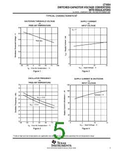
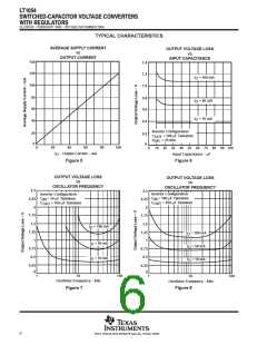
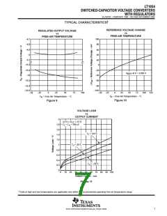
ꢀ
ꢁ
ꢂ
ꢃ
ꢄ
ꢅ
ꢆ
ꢆ
ꢆꢇ ꢈ ꢁꢉ ꢊꢋꢌꢍꢉ ꢎꢏꢎꢉꢈ ꢁꢐ ꢑ ꢒꢐ ꢀꢁꢎꢓ ꢋ ꢉꢐ ꢔ ꢒꢋ ꢑꢁ ꢋꢑ
ꢇ ꢈꢁ ꢊ ꢑꢋꢓ ꢕ ꢀꢎꢁꢐ ꢑ
SLVS033F − FEBRUARY 1990 − REVISED NOVEMBER 2004
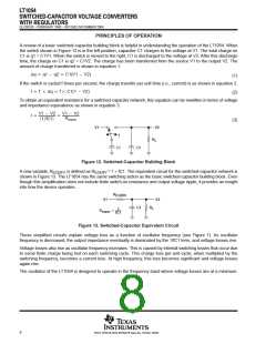
PRINCIPLES OF OPERATION
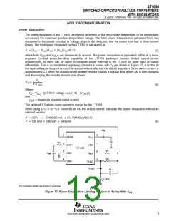
Supply voltage V
and then transfers charge to C
frequency. During the time that C is charging, the peak supply current is approximately 2.2 times the output current.
During the time that C is delivering a charge to C
alternately charges C to the input voltage when C is switched in parallel with the input supply
IN IN
CC
when C is switched in parallel with C
. Switching occurs at the oscillator
OUT
IN
OUT
IN
, the supply current drops to approximately 0.2 times the output
IN
OUT
current. An input supply bypass capacitor supplies part of the peak input current drawn by the LT1054 and averages
the current drawn from the supply. A minimum input-supply bypass capacitor of 2 µF, preferably tantalum or some
other low equivalent-series-resistance (ESR) type, is recommended. A larger capacitor is desirable in some cases.
An example of this would be when the actual input supply is connected to the LT1054 through long leads or when
the pulse currents drawn by the LT1054 might affect other circuits through supply coupling.
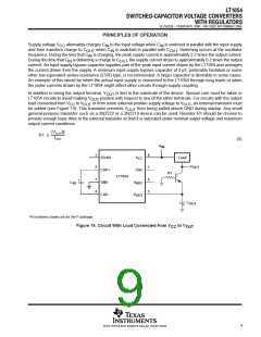
In addition to being the output terminal, V
is tied to the substrate of the device. Special care must be taken in
OUT
LT1054 circuits to avoid making V
positive with respect to any of the other terminals. For circuits with the output
or from some external positive supply voltage to V
OUT
load connected from V
to V
, an external transistor must
CC
OUT
OUT
be added (see Figure 14). This transistor prevents V
from being pulled above GND during startup. Any small
OUT
general-purpose transistor such as a 2N2222 or a 2N2219 device can be used. Resistor R1 should be chosen to
provide enough base drive to the external transistor so that it is saturated under nominal output voltage and maximum
output current conditions.
Ť
Ť
Ǔ
b
ǒ
VOUT
R1 v
IOUT
(4)
V
IN
1
2
8
7
6
5
FB/SD
CAP+
GND
V
Load
CC
V
OUT
OSC
R1
LT1054
3
4
+
C
V
REF
IN
CAP−
V
OUT
C
OUT
+
Pin numbers shown are for the P package.
Figure 14. Circuit With Load Connected from V
to V
OUT
CC
9
POST OFFICE BOX 655303 • DALLAS, TEXAS 75265

 TI [ TEXAS INSTRUMENTS ]