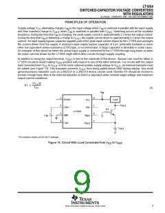
ꢀ
ꢁ
ꢂ
ꢃ
ꢄ
ꢅ
ꢆ
ꢆ
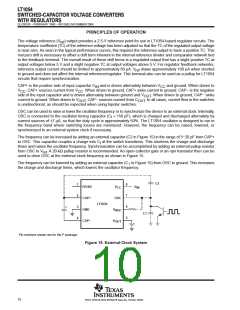
ꢆꢇ ꢈ ꢁꢉ ꢊꢋꢌꢍꢉ ꢎꢏꢎꢉꢈ ꢁꢐ ꢑ ꢒꢐ ꢀꢁꢎꢓ ꢋ ꢉꢐ ꢔ ꢒꢋ ꢑꢁ ꢋꢑ
ꢇ ꢈꢁ ꢊ ꢑꢋꢓ ꢕ ꢀꢎꢁꢐ ꢑ
SLVS033F − FEBRUARY 1990 − REVISED NOVEMBER 2004
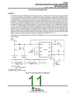
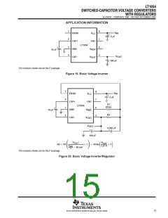
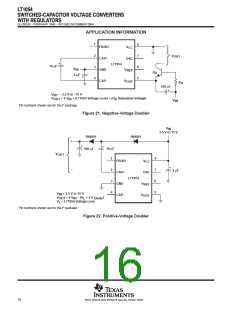
APPLICATION INFORMATION
power dissipation
The power dissipation of any LT1054 circuit must be limited so that the junction temperature of the device does
not exceed the maximum junction-temperature ratings. The total power dissipation is calculated from two
components–the power loss due to voltage drops in the switches, and the power loss due to drive-current
losses. The total power dissipated by the LT1054 is calculated as:
Ť
Ť
Ǔ
ǒ
ǒ
Ǔǒ
Ǔ
(
)
P [ VCC * VOUT IOUT ) VCC IOUT 0.2
(7)
where both V and V are referenced to ground. The power dissipation is equivalent to that of a linear
CC
OUT
regulator. Limited power-handling capability of the LT1054 packages causes limited output-current
requirements, or steps can be taken to dissipate power external to the LT1054 for large input or output
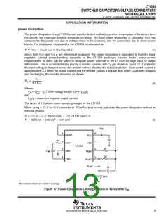
differentials. This is accomplished by placing a resistor in series with C as shown in Figure 17. A portion of
IN
the input voltage is dropped across this resistor without affecting the output regulation. Since switch current is
approximately 2.2 times the output current and the resistor causes a voltage drop when C is both charging
IN
and discharging, the resistor chosen is as shown:
VX
4.4 IOUT
RX +
(8)
Where:
V
≈ V
− [(LT1054 voltage loss)(1.3) + |V
|]
OUT
X
CC
and
I
= maximum required output current
OUT
The factor of 1.3 allows some operating margin for the LT1054.
When using a 12-V to −5-V converter at 100-mA output current, calculate the power dissipation without an
external resistor.
(
|
|)(
)
(
)(
)(
)
P + 12 V * *5 V 100 mA ) 12 V 100 mA 0.2
P + 700 mW ) 240 mW + 940 mW
(9)
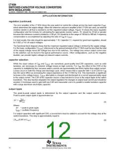
V
IN
1
8
7
6
5
FB/SD
CAP+
GND
V
CC
Rx
2
3
4
OSC
LT1054
R1
R2
+
C
V
REF
IN
CAP−
V
OUT
V
OUT
C1
C
OUT
+
Pin numbers shown are for the P package.
Figure 17. Power-Dissipation-Limiting Resistor in Series With C
IN
13
POST OFFICE BOX 655303 • DALLAS, TEXAS 75265

 TI [ TEXAS INSTRUMENTS ]