ꢀꢁ ꢂꢃ ꢄꢅ
ꢆ ꢇꢈ ꢁ ꢉꢊ ꢋꢌ ꢍꢉ ꢎ ꢏꢎꢉ ꢈ ꢁꢐ ꢑ ꢒ ꢐꢀꢁꢎꢓ ꢋ ꢉꢐ ꢔ ꢒꢋꢑꢁ ꢋ ꢑꢆ
ꢇꢈ ꢁ ꢊ ꢑ ꢋꢓꢕ ꢀ ꢎꢁꢐ ꢑꢆ
SLVS033F − FEBRUARY 1990 − REVISED NOVEMBER 2004
APPLICATION INFORMATION
regulation (continued)
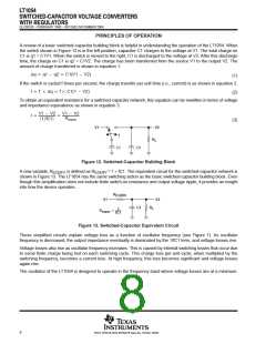
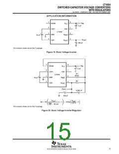
The error amplifier of the LT1054 drives the pnp switch to control the voltage across the input capacitor (C ),
IN
which determines the output voltage. When the reference and error amplifier of the LT1054 are used, an external
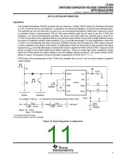
resistive divider is all that is needed to set the regulated output voltage. Figure 16 shows the basic regulator
configuration and the formula for calculating the appropriate resistor values. R1 should be 20 kΩ or greater
because the reference current is limited to 100 µA. R2 should be in the range of 100 kΩ to 300 kΩ. Frequency
compensation is accomplished by adjusting the ratio of C to C
IN
OUT.
For best results, this ratio should be approximately 1:10. Capacitor C1, required for good load regulation, should
be 0.002 µF for all output voltages.
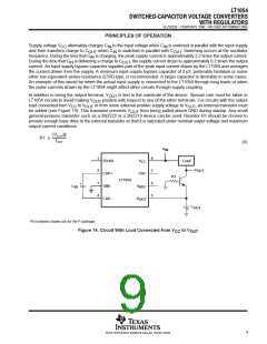
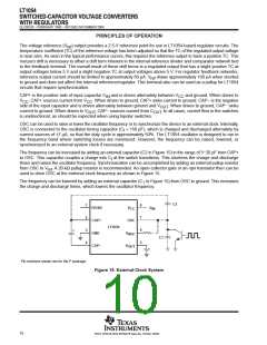
The functional block diagram shows that the maximum regulated output voltage is limited by the supply voltage.
For the basic configuration, V
referenced to the ground terminal of the LT1054 must be less than the total
OUT
of the supply voltage minus the voltage loss due to the switches. The voltage loss versus output current due
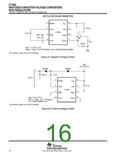
to the switches can be found in the typical performance curves. Other configurations, such as the negative
doubler, can provide higher voltages at reduced output currents.
capacitor selection
While the exact values of C and C
tantalum, are necessary to minimize voltage losses at high currents. For C , the effect of the ESR of the
capacitor is multiplied by four, because switch currents are approximately two times higher than output current.
are noncritical, good-quality low-ESR capacitors, such as solid
IN
OUT
IN
Losses occur on both the charge and discharge cycle, which means that a capacitor with 1 Ω of ESR for C
IN
has the same effect as increasing the output impedance of the LT1054 by 4 Ω. This represents a significant
increase in the voltage losses. C alternately is charged and discharged at a current approximately equal
OUT
to the output current. The ESR of the capacitor causes a step function to occur in the output ripple at the switch
transitions. This step function degrades the output regulation for changes in output load current and should be
avoided. A technique used to gain both low ESR and reasonable cost is to parallel a smaller tantalum capacitor
with a large aluminum electrolytic capacitor.
output ripple
The peak-to-peak output ripple is determined by the output capacitor and the output current values.
Peak-to-peak output ripple is approximated as:
IOUT
2fCOUT
DV +
(5)
Where:
∆V = peak-to-peak ripple
= oscillator frequency
f
OSC
For output capacitors with significant ESR, a second term must be added to account for the voltage step at the
switch transitions. This step is approximately equal to:
ǒ
Ǔǒ Ǔ
2IOUT ESR of COUT
(6)
12
POST OFFICE BOX 655303 • DALLAS, TEXAS 75265

 TI [ TEXAS INSTRUMENTS ]