ꢀ
ꢁ
ꢂ
ꢃ
ꢄ
ꢅ
ꢆ
ꢆ
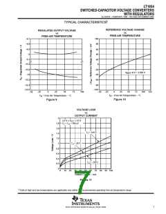
ꢆꢇ ꢈ ꢁꢉ ꢊꢋꢌꢍꢉ ꢎꢏꢎꢉꢈ ꢁꢐ ꢑ ꢒꢐ ꢀꢁꢎꢓ ꢋ ꢉꢐ ꢔ ꢒꢋ ꢑꢁ ꢋꢑ
ꢇ ꢈꢁ ꢊ ꢑꢋꢓ ꢕ ꢀꢎꢁꢐ ꢑ
SLVS033F − FEBRUARY 1990 − REVISED NOVEMBER 2004
APPLICATION INFORMATION
regulation
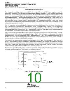
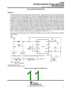
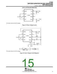
The feedback/shutdown (FB/SD) terminal has two functions. Pulling FB/SD below the shutdown threshold
(≈ 0.45 V) puts the device into shutdown. In shutdown, the reference/regulator is turned off and switching stops.
The switches are set such that both C and C
are discharged through the output load. Quiescent current
IN
OUT
in shutdown drops to approximately 100 µA. Any open-collector gate can be used to put the LT1054 into
shutdown. For normal (unregulated) operation, the device will restart when the external gate is shut off. In
LT1054 circuits that use the regulation feature, the external resistor divider can provide enough pulldown to keep
the device in shutdown until the output capacitor (C
) has fully discharged. For most applications, where the
OUT
LT1054 is run intermittently, this does not present a problem because the discharge time of the output capacitor
is short compared to the off time of the device. In applications where the device has to start up before the output
capacitor (C
) has fully discharged, a restart pulse must be applied to FB/SD of the LT1054. Using the circuit
OUT
shown in Figure 16, the restart signal can be either a pulse (t > 100 µs) or a logic high. Diode coupling the restart
p
signal into FB/SD allows the output voltage to rise and regulate without overshoot. The resistor divider R3/R4
shown in Figure 16 should be chosen to provide a signal level at FB/SD of 0.7−1.1 V.
FB/SD also is the inverting input of the LT1054 error amplifier and, as such, can be used to obtain a regulated
output voltage.
R3
R4
V
IN
2.2 µF
1
2
3
4
8
7
6
5
+
FB/SD
CAP+
GND
V
CC
OSC
LT1054
C
10-µF
Tantalum
IN
R1
R2
+
V
REF
CAP−
V
OUT
Restart
Shutdown
V
OUT
C1
For example: To get V = −5 V, referenced to the ground terminal of the LT1054
O
Ť
Ť
VOUT
C
|
|
–5 V
OUT
100-µF
Tantalum
†
R2 + R1
) 1 + 20 kW
) 1
+ 102.6 kW
ǒ Ǔ ǒ Ǔ
V
2.5 V
REF * 40 mV
* 40 mV
+
2
2
Where: R1 = 20 kΩ
V
= 2.5 V Nominal
REF
Choose the closest 1% value.
Pin numbers shown are for the P package.
†
Figure 16. Basic Regulation Configuration
11
POST OFFICE BOX 655303 • DALLAS, TEXAS 75265

 TI [ TEXAS INSTRUMENTS ]