LMH0324
www.ti.com.cn
ZHCSIC8B –APRIL 2016–REVISED JUNE 2018
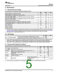
6 Specifications
6.1 Absolute Maximum Ratings
over operating free-air temperature range (unless otherwise noted)(1)
MIN
–0.5
–0.5
MAX
2.75
2.0
UNIT
V
Supply Voltage for 2.5-V Mode (VIN, VDDIO)
Supply Voltage for 1.8-V Mode (VIN, VDD_LDO, VDDIO)
V
4-Level Input/Output Voltage for 2.5 V Supply (IN_OUT_SEL, OUT_CTRL, VOD_DE,
MODE_SEL, ADDR0, ADDR1)
–0.5
-0.5
2.75
2.0
V
V
4-Level Input/Output Voltage for 1.8 V Supply (IN_OUT_SEL, OUT_CTRL, VOD_DE,
MODE_SEL, ADDR0, ADDR1)
SMBus Input/Output Voltage (SDA, SCL)(2)
SPI Input/Output Voltage for 2.5 V Supply (SS_N, MISO, MOSI, and SCK)
SPI Input/Output Voltage for 1.8 V Supply (SS_N, MISO, MOSI, and SCK)
Input Voltage (IN0±)
–0.5
–0.5
-0.5
–0.5
–30
4.0
2.75
2.0
V
V
V
2.75
30
V
Input Current (IN0±)
mA
°C
°C
Junction Temperature
125
150
Storage temperature
-65
(1) Stresses beyond those listed under Absolute Maximum Ratings may cause permanent damage to the device. These are stress ratings
only, which do not imply functional operation of the device at these or any other conditions beyond those indicated under Recommended
Operating Conditions. Exposure to absolute-maximum-rated conditions for extended periods may affect device reliability.
(2) SDA and SCL is 3.3 V tolerant when VDDIO is 2.5 V.
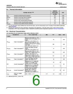
6.2 ESD Ratings
VALUE
±4500
±1500
UNIT
Human-body model (HBM), per ANSI/ESDA/JEDEC JS-001(1)
Charged-device model (CDM), per JEDEC specification JESD22-C101(2)
V(ESD) Electrostatic discharge
V
(1) JEDEC document JEP155 states that 500 V HBM allows safe manufacturing with a standard ESD control process. Manufacturing with
less than 500 V HBM is possible with the necessary precautions. Pins listed as ±4500 V may actually have higher performance.
(2) JEDEC document JEP157 states that 250 V CDM allows safe manufacturing with a standard ESD control process. Manufacturing with
less than 250 V CDM is possible with the necessary precautions. Pins listed as ±1500 V may actually have higher performance.
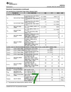
6.3 Recommended Operating Conditions
over operating free-air temperature range (unless otherwise noted)
MIN
2.375
1.71
NOM
2.5
MAX
2.625
1.89
3.6
UNIT
2.5 V Supplies
1.8 V Supplies
VDDSMBUS
VIN, VDDIO to VSS
V
V
V
VIN, VDDIO , VDD_LDO to VSS
SMBus: SDA, SCL Open Drain Termination Voltage, VDDIO = 2.5 V
Source Launch Amplitude before Coax
Splitter Mode
1.8
2.375
0.72
0.8
0.4
0.88
0.44
100
VLAUNCH
Vp-p
0.36
TJUNCTION
TAMBIENT
Operating Junction Temperature
Ambient Temperature
°C
°C
–40
25
85
50 Hz to 1 MHz, Sinusoidal
<20
(1)
NPS
Supply Noise
mVp-p
1.1 MHz to 6 GHz,
Sinusoidal
<10
(1) The sum of the DC supply voltage and AC supply noise should not exceed the recommended supply voltage range.
Copyright © 2016–2018, Texas Instruments Incorporated
5

 TI [ TEXAS INSTRUMENTS ]