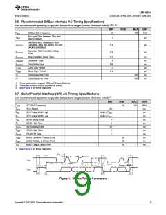
LMH0324
ZHCSIC8B –APRIL 2016–REVISED JUNE 2018
www.ti.com.cn
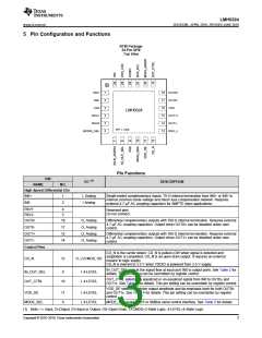
Pin Functions (continued)
PIN
(1)
I/O
DESCRIPTION
NAME
NO.
Serial Control Interface (SPI Mode), MODE_SEL = F (Float)
SS_N is the Slave Select. When SS_N is at logic Low, it enables SPI access to the
LMH0324 slave device. SS_N is a LVCMOS input referenced to VDDIO.
SS_N
MISO
MOSI
SCK
7
I, LVCMOS
O, LVCMOS
I, LVCMOS
I, LVCMOS
MISO is the SPI serial data output from the LMH0324 slave device. MISO is a
LVCMOS output referenced to VDDIO.
20
10
21
MOSI is used as the SPI serial data input to the LMH0324 slave device. MOSI is
LVCMOS input referenced to VDDIO.
SCK is the SPI serial input clock to the LMH0324 slave device. SCK is LVCMOS
referenced to VDDIO.
Serial Control Interface (SMBus MODE) , MODE_SEL = L (1 kΩ to VSS)
ADDR0
ADDR1
7
Strap, 4-LEVEL
Strap, 4-LEVEL
ADDR[1:0] are SMBus address straps to select one of the 16 supported SMBus
addresses. ADDR[1:0] are 4-level straps and are read into the device at power up.
20
SMBus bi-directional open drain data line to or from the LMH0324 slave device. SDA
is an open drain IO and requires an external 2 kΩ to 5 kΩ pull-up resistor to the
SMBus termination voltage. SDA is 3.3 V tolerant when VDDIO is powered from 2.5
V.
SDA
SCL
10
21
IO, LVCMOS, OD
I, LVCMOS, OD
SMBus input clock to the LMH0324 slave device. It is driven by a LVCMOS open
drain driver from the SMBus master. SCL requires an external 2 kΩ to 5 kΩ pull-up
resistor to the SMBus termination voltage. SCL is 3.3 V tolerant when VDDIO is
powered from 2.5 V.
Power
VSS
3, 9, 16
24
I, Ground
I, Power
Ground reference.
VIN is connected to an external power supply. It accepts either 2.5 V ± 5% or 1.8 V ±
5%. When VIN is powered from 2.5 V, VDD_LDO is the output of an on-chip LDO
regulator and requires a bypass capacitor to VSS.
VIN
When VIN is powered from 1.8 V, for lower power operation, both VIN and VDD_LDO
should be connected to 1.8 V supply.
VDDIO powers the LVCMOS IO and 4-level input logic. VDDIO should be connected
to 2.5 V ± 5% or 1.8 V ± 5%. VDDIO must always be greater than or equal to VIN.
For SMBus access, VDDIO must be 2.5 V ± 5%.
VDDIO
22
23
I, Power
VDD_LDO is the output of the internal 1.8 V LDO regulator when VIN is connected to
2.5 V supply. VDD_LDO output requires external 1-µF and 0.1-µF bypass capacitors
to VSS. The internal LDO is designed to power internal circuitry only. VDD_LDO is an
input when VIN is powered from 1.8 V for lower power operation. When VIN is
connected to a 1.8 V supply, both VIN and VDD_LDO should be connected to the 1.8
V supply.
VDD_LDO
IO, Power
For pin compatibility with the LMH1219 (11.88 Gbps Ultra-HD adaptive cable
equalizer with integrated reclocker), connect RSV_L to a 2.5 V supply with a 0.1-µF
bypass capacitor. For low power operation, tie RSV_L to VSS. See Power Supply
Recommendations for details.
RSV_L
EP
13
I
EP is the exposed pad at the bottom of the QFN package. The exposed pad must be
connected to the ground plane through a via array. See 图 26 for details.
I, Ground
4
Copyright © 2016–2018, Texas Instruments Incorporated

 TI [ TEXAS INSTRUMENTS ]