LMH0324
www.ti.com.cn
ZHCSIC8B –APRIL 2016–REVISED JUNE 2018
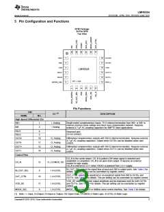
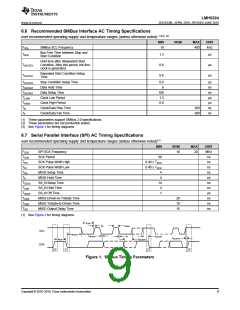
5 Pin Configuration and Functions
RTW Package
24-Pin QFN
Top View
IN0+
IN0-
1
2
3
4
5
6
18 OUT0+
17 OUT0-
16 VSS
VSS
LMH0324
RSV1
15 OUT1+
14 OUT1-
13 RSV_L
RSV2
EP = VSS
MODE_SEL
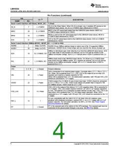
Pin Functions
PIN
(1)
I/O
DESCRIPTION
NAME
NO.
High Speed Differential I/Os
IN0+
IN0-
1
2
I, Analog
I Analog
Single-ended complementary inputs, 75-Ω internal termination from IN0+ or IN0- to
internal common mode voltage and return loss compensation network. Requires
external 4.7-µF AC coupling capacitors for SMPTE video applications.
RSV1
RSV2
OUT0+
4
5
Reserved pins.
Do not connect.
18
O, Analog
O, Analog
O, Analog
O, Analog
Differential complementary outputs with 100-Ω internal termination. Requires external
4.7-µF AC coupling capacitors. Output driver OUT0± can be disabled under user
control.
OUT0-
17
15
14
OUT1+
Differential complementary outputs with 100-Ω internal termination. Requires external
4.7-µF AC coupling capacitors. Output driver OUT1± can be disabled under user
control.
OUT1-
Control Pins
CD_N is the carrier detect. CD_N is pulled LOW when signal is detected and
adaptation is completed. CD_N is an open drain output. It requires an external
resistor to logic supply.
CD_N
12
O, LVCMOS, OD
CD_N is tolerant to 3.3 V when VDDIO is powered from 2.5 V supply.
IN_OUT_SEL selects the signal flow at input port IN0 to output ports. See Table 2 for
details. This pin setting can be overridden by register control.
IN_OUT_SEL
OUT_CTRL
8
I, 4-LEVEL
I, 4-LEVEL
OUT_CTRL selects the equalized or un-equalized signal from IN0 to OUT0± and
OUT1±. See Table 3 for details. This pin setting can be overridden by register control.
19
VOD_DE selects the driver output amplitude and de-emphasis level for both OUT0±
and OUT1±. See Table 4 for details. This pin setting can be overridden by register
control.
VOD_DE
11
6
I, 4-LEVEL
I, 4-LEVEL
MODE_SEL
MODE_SEL enables SPI or SMBus serial control interface. See Table 5 for details.
(1) Note: I = Input, O=Output, IO=Input or Output, OD=Open Drain, LVCMOS=2-State Logic, 4-LEVEL=4-State Logic
Copyright © 2016–2018, Texas Instruments Incorporated
3

 TI [ TEXAS INSTRUMENTS ]