LM5116
www.ti.com
SNVS499G –FEBRUARY 2007–REVISED MARCH 2013
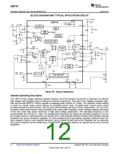
High Voltage Start-Up Regulator
The LM5116 contains a dual mode internal high voltage startup regulator that provides the VCC bias supply for
the PWM controller and a boot-strap gate drive for the high-side buck MOSFET. The input pin (VIN) can be
connected directly to an input voltage source as high as 100 volts. For input voltages below 10.6V, a low dropout
switch connects VCC directly to VIN. In this supply range, VCC is approximately equal to VIN. For VIN voltages
greater than 10.6V, the low dropout switch is disabled and the VCC regulator is enabled to maintain VCC at
approximately 7.4V. The wide operating range of 6V to 100V is achieved through the use of this dual mode
regulator.
Upon power-up, the regulator sources current into the capacitor connected to the VCC pin. When the voltage at
the VCC pin exceeds 4.5V and the UVLO pin is greater than 1.215V, the output switch is enabled and a soft-start
sequence begins. The output switch remains enabled until VCC falls below 4.5V, EN is pulled low, the UVLO pin
falls below 1.215V or the die temperature exceeds the thermal limit threshold.
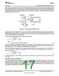
VCCX
C
VCCX
V
OUT
SW
L
C
OUT
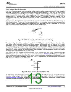
Figure 27. VCCX Bias Supply with Additional Inductor Winding
An output voltage derived bias supply can be applied to the VCCX pin to reduce the IC power dissipation. If the
bias supply voltage is greater than 4.5V, the internal regulator will essentially shut off, reducing the IC power
dissipation. The VCC regulator series pass transistor includes a diode between VCC and VIN that should not be
forward biased in normal operation. For an output voltage between 5V and 15V, VOUT can be connected directly
to VCCX. For VOUT < 5V, a bias winding on the output inductor can be added to VOUT. If the bias winding can
supply VCCX greater than VIN, an external blocking diode is required from the input power supply to the VIN pin
to prevent VCC from discharging into the input supply.
The output of the VCC regulator is current limited to 15 mA minimum. The VCC current is determined by the
MOSFET gate charge, switching frequency and quiescent current (see MOSFETs). If VCCX is powered by the
output voltage or an inductor winding, the VCC current should be evaluated during startup to ensure that it is less
than the 15 mA minimum current limit specification. IF VCCX is powered by an external regulator derived from
VIN, there is no restriction on the VCC current.
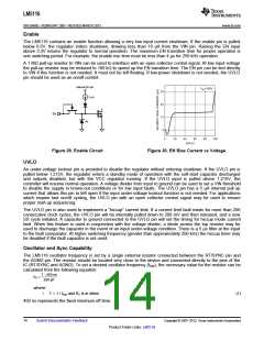
V
IN
1
6
VIN
0.1 mF
AGND
Figure 28. Input Blocking Diode for VCCX > VIN
In high voltage applications extra care should be taken to ensure the VIN pin does not exceed the absolute
maximum voltage rating of 100V. During line or load transients, voltage ringing on the VIN line that exceeds the
Absolute Maximum Ratings can damage the IC. Both careful PC board layout and the use of quality bypass
capacitors located close to the VIN and GND pins are essential.
Copyright © 2007–2013, Texas Instruments Incorporated
Submit Documentation Feedback
13
Product Folder Links: LM5116

 TI [ TEXAS INSTRUMENTS ]