LM3410, LM3410Q
www.ti.com
SNVS541G –OCTOBER 2007–REVISED MAY 2013
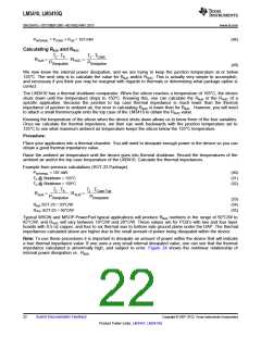
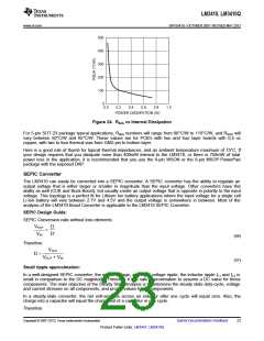
Figure 24. RθJA vs Internal Dissipation
For 5-pin SOT-23 package typical applications, RθJA numbers will range from 80°C/W to 110°C/W, and RΨJC will
vary between 50°C/W and 65°C/W. These values are for PCB’s with two and four layer boards with 0.5 oz
copper, with two to four thermal vias from GND pin to bottom layer.
Here is a good rule of thumb for typical thermal impedances, and an ambient temperature maximum of 75°C: If
your design requires that you dissipate more than 400mW internal to the LM3410, or there is 750mW of total
power loss in the application, it is recommended that you use the 6-pin WSON or the 8-pin MSOP-PowerPad
package with the exposed DAP.
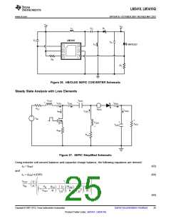
SEPIC Converter
The LM3410 can easily be converted into a SEPIC converter. A SEPIC converter has the ability to regulate an
output voltage that is either larger or smaller in magnitude than the input voltage. Other converters have this
ability as well (CUK and Buck-Boost), but usually create an output voltage that is opposite in polarity to the input
voltage. This topology is a perfect fit for Lithium Ion battery applications where the input voltage for a single cell
Li-Ion battery will vary between 2.7V and 4.5V and the output voltage is somewhere in between. Most of the
analysis of the LM3410 Boost Converter is applicable to the LM3410 SEPIC Converter.
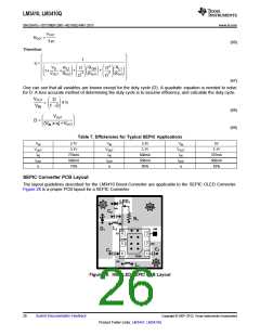
SEPIC Design Guide:
SEPIC Conversion ratio without loss elements:
VOUT
VIN
D
=
D‘
(56)
(57)
Therefore:
VOUT
D =
VOUT + VIN
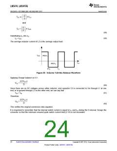
Small ripple approximation:
In a well-designed SEPIC converter, the output voltage, and input voltage ripple, the inductor ripple IL1 and IL2 is
small in comparison to the DC magnitude. Therefore it is a safe approximation to assume a DC value for these
components. The main objective of the Steady State Analysis is to determine the steady state duty-cycle, voltage
and current stresses on all components, and proper values for all components.
In a steady-state converter, the net volt-seconds across an inductor after one cycle will equal zero. Also, the
charge into a capacitor will equal the charge out of a capacitor in one cycle.
Therefore:
Copyright © 2007–2013, Texas Instruments Incorporated
Submit Documentation Feedback
23
Product Folder Links: LM3410 LM3410Q

 TI [ TEXAS INSTRUMENTS ]