LM3410, LM3410Q
SNVS541G –OCTOBER 2007–REVISED MAY 2013
www.ti.com
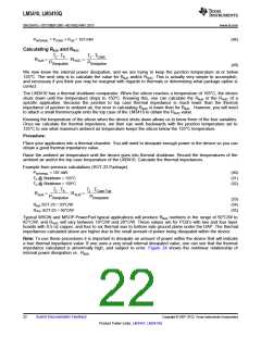
VOUT
ROUT
=
ILED
(66)
Therefore:
≈
’
÷
∆
1
∆
÷
÷
÷
÷
h =
∆
∆
∆
2
2
≈
∆
’
÷
≈
∆
’
÷
≈
∆
«
VD
’
÷
÷
R
R
L1
RL2
D
2
≈
∆
’
÷
D
≈
’
ON
+
+
∆
÷
1+
+
∆
∆
«
÷
◊
∆
«
÷
◊
VOUT ROUT
'
ROUT
'
ROUT
« ◊
«
◊
◊
D
D
∆
«
÷
◊
(67)
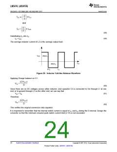
One can see that all variables are known except for the duty cycle (D). A quadratic equation is needed to solve
for D. A less accurate method of determining the duty cycle is to assume efficiency, and calculate the duty cycle.
VOUT
≈
’
÷
D
x h
=
∆
VIN
1 - D
«
◊
(68)
(69)
VOUT
’
÷
◊
≈
D =
∆
(V x h) +VOUT
IN
«
Table 7. Efficiencies for Typical SEPIC Applications
VIN
VOUT
IIN
2.7V
3.1V
VIN
VOUT
IIN
3.3V
3.1V
VIN
VOUT
IIN
5V
3.1V
770mA
500mA
75%
600mA
500mA
80%
375mA
500mA
83%
ILED
η
ILED
η
ILED
η
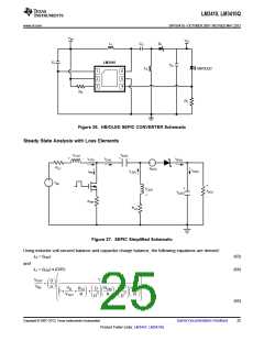
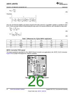
SEPIC Converter PCB Layout
The layout guidelines described for the LM3410 Boost-Converter are applicable to the SEPIC OLED Converter.
Figure 28 is a proper PCB layout for a SEPIC Converter.
LED1
VO
PGND
C2
R1
L2
FB
DIM
D1
4
3
2
1
AGND
5
VIN
C1
C3
6
PGND
SW
VIN
L1
Figure 28. HB/OLED SEPIC PCB Layout
26
Submit Documentation Feedback
Copyright © 2007–2013, Texas Instruments Incorporated
Product Folder Links: LM3410 LM3410Q

 TI [ TEXAS INSTRUMENTS ]